Method for preparing organic semiconductor single crystal micro-nano wire array by brush
A technology of organic semiconductors and micro-nano wires, applied in the field of organic electronics, can solve the problems of uncontrollable direction and position of micro-nano wires, difficulty in growing micro-nano wire arrays, low success rate of micro-nano wire arrays, etc. Area preparation, process and equipment are simple, and the effect of gravity is small
- Summary
- Abstract
- Description
- Claims
- Application Information
AI Technical Summary
Problems solved by technology
Method used
Image


Examples
Embodiment 1
[0043] Embodiment 1, on the rigid substrate of plane (silicon chip, silicon / silicon dioxide chip, glass sheet etc.), utilize writing brush to control growth TCNQ micro-nano line array
[0044] (1) Clean silicon wafers, silicon / silicon dioxide wafers or glass substrates according to the following steps: Ultrasonic in acetone solution for 15 minutes, and dry on filter paper; then soak in chromic acid washing solution for 10 minutes, and then Rinse with deionized water and blow dry with general nitrogen.
[0045] Then, the above-mentioned substrate was subjected to plasma treatment in an oxygen atmosphere for 2 minutes, the power was 40W, the vacuum degree was 36 Pa, and the flow rate of oxygen was 8 sccm.
[0046] (2) The organic semiconductor TCNQ powder was dissolved in acetonitrile solvent, and a solution with a concentration of 0.8 g / L was prepared.
[0047] (3) Under atmospheric conditions, use a brush to dip the solution obtained in step (2), and then apply it to the plac...
Embodiment 2
[0050] Embodiment 2. On flexible or curved substrates (polyethylene terephthalate film (PET), three-dimensional glass hemispheres and contact lenses, etc.), use a brush to control the growth of TCNQ micro-nano line arrays
[0051] (1) Clean the three-dimensional glass hemispherical substrate according to the following steps: Ultrasound in acetone solution for 15 minutes, and dry on filter paper; then soak in chromic acid lotion for 10 minutes, rinse with deionized water, and then wash with ordinary Blow dry with nitrogen.
[0052] Follow the steps below to clean the polyethylene terephthalate film: first use acetone and ethanol to ultrasonically, then blow dry with general nitrogen;
[0053] Follow the steps below to clean contact lenses: clean the contact lens lotion, and then dry the upper surface with general nitrogen;
[0054] Then, the above-mentioned substrate was subjected to plasma treatment in an oxygen atmosphere for 2 minutes, the power was 40W, the vacuum degree w...
Embodiment 3
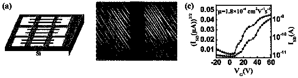
[0059] Embodiment 3, in SiO 2 On the / Si sheet substrate, the TCNQ micro-nano line array obtained in embodiment 1 is used as a semiconductor layer to prepare a field-effect transistor and its performance test
[0060] (1) cleaning SiO2 2 / Si substrate;
[0061] (2) Utilize technologies such as photolithography and evaporation to prepare patterned source-drain Au electrodes on the substrate obtained in step (1);
[0062] (3) On the substrate obtained in step (2), use the TCNQ micro-nano wire array obtained in Example 1 as the semiconductor layer of the transistor.
[0063] (4) For Si with a thickness of 450 μm as the gate, Au with a thickness of 30 nm as the source and drain electrodes, and SiO with a thickness of 300 nm 2 It is an insulating layer, and the TCNQ micro-nano wire array is a field-effect transistor prepared from a semiconductor. The transfer curve is tested under normal temperature and atmospheric conditions.
[0064] (5) Using the saturation zone formula Ca...
PUM
| Property | Measurement | Unit |
|---|---|---|
| concentration | aaaaa | aaaaa |
| width | aaaaa | aaaaa |
| thickness | aaaaa | aaaaa |
Abstract
Description
Claims
Application Information
 - R&D
- Intellectual Property
- Life Sciences
- Materials
- Tech Scout
- Unparalleled Data Quality
- Higher Quality Content
- 60% Fewer Hallucinations
Browse by: Latest US Patents, China's latest patents, Technical Efficacy Thesaurus, Application Domain, Technology Topic, Popular Technical Reports.
© 2025 PatSnap. All rights reserved.Legal|Privacy policy|Modern Slavery Act Transparency Statement|Sitemap|About US| Contact US: help@patsnap.com