GaN-based double heterojunction HEMT (High Electron Mobility Transistor) device and manufacturing method thereof
A double heterojunction and device technology, which is applied in semiconductor/solid-state device manufacturing, semiconductor devices, electrical components, etc., can solve the problems of microwave output current drop, device saturation voltage drop, and device switching ratio reduction, so as to reduce the mixed crystal Effects of scattering, reducing parasitic conductance and leakage current, increasing concentration
- Summary
- Abstract
- Description
- Claims
- Application Information
AI Technical Summary
Problems solved by technology
Method used
Image

Examples
Embodiment 1
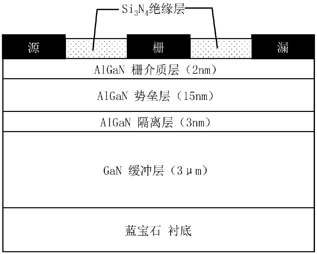
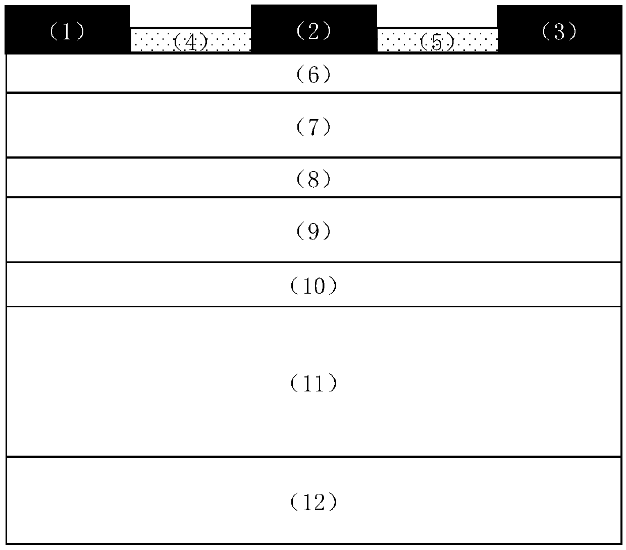
[0035] see figure 2 , which is a schematic diagram of the structure of the GaN-based double heterojunction high electron mobility transistor device of the present invention. In the preparation process, sapphire was used as the substrate, trimethylgallium (TMGa), trimethylaluminum (TMAl), and trimethylindium (TMIn) were used as gallium sources, aluminum sources, and indium sources, respectively, and high-purity ammonia gas was used as the source. Nitrogen source, hydrogen as carrier gas, the specific preparation process is as follows:
[0036] 1. Place the sapphire substrate in the reaction chamber of the metal-organic chemical vapor deposition (MOCVD) equipment, and evacuate the vacuum of the reaction chamber to 1×10 -2 Below Torr, the sapphire substrate is subjected to high-temperature heat treatment under the protection of hydrogen, the heating temperature is 1100°C, the heating time is 5min, the pressure of the reaction chamber is 40Torr, and the flow rate of hydrogen gas...
Embodiment 2
[0051] see figure 2 , which is a schematic diagram of the structure of the GaN-based double heterojunction high electron mobility transistor device of the present invention. In the preparation process, sapphire was used as the substrate, trimethylgallium (TMGa), trimethylaluminum (TMAl), and trimethylindium (TMIn) were used as gallium sources, aluminum sources, and indium sources, respectively, and high-purity ammonia gas was used as the source. Nitrogen source, hydrogen as carrier gas, the specific preparation process is as follows:
[0052] 1. Place the sapphire substrate in the reaction chamber of the metal-organic chemical vapor deposition (MOCVD) equipment, and evacuate the vacuum of the reaction chamber to 1×10 -2 Below Torr, the sapphire substrate is subjected to high-temperature heat treatment under the protection of hydrogen, the heating temperature is 1100°C, the heating time is 5min, the pressure of the reaction chamber is 40Torr, and the flow rate of hydrogen gas...
Embodiment 3
[0067] see figure 2 , which is a schematic diagram of the structure of the GaN-based double heterojunction high electron mobility transistor device of the present invention. In the preparation process, sapphire was used as the substrate, trimethylgallium (TMGa), trimethylaluminum (TMAl), and trimethylindium (TMIn) were used as gallium sources, aluminum sources, and indium sources, respectively, and high-purity ammonia gas was used as the source. Nitrogen source, hydrogen as carrier gas, the specific preparation process is as follows:
[0068] 1. Place the sapphire substrate in the reaction chamber of the metal-organic chemical vapor deposition (MOCVD) equipment, and evacuate the vacuum of the reaction chamber to 1×10 -2 Below Torr, the sapphire substrate is subjected to high-temperature heat treatment under the protection of hydrogen, the heating temperature is 1100°C, the heating time is 5min, the pressure of the reaction chamber is 40Torr, and the flow rate of hydrogen gas...
PUM
 Abstract
Description
Claims
Application Information