SiC annular floating-point type P+ structured junction barrier Schottky diode and preparation method thereof

A junction-barrier Schottky and floating-point technology, used in semiconductor/solid-state device manufacturing, electrical components, circuits, etc. The effect of conducting conduction current, increasing conduction path, and increasing contact area

Inactive Publication Date: 2016-06-29
JIANGSU JIEJIE MICROELECTRONICS
View PDF6 Cites 9 Cited by
  • Summary
  • Abstract
  • Description
  • Claims
  • Application Information

AI Technical Summary

Problems solved by technology

However, at low voltage, since the SiCpn junction is not open, the conduction current is mainly completed by the Schottky contact. The introduction of the strip P+ junction will reduce the forward conduction current of the device and increase the conduction resistance (such as figure 1 and figure 2 shown)

Method used


Image

  • SiC annular floating-point type P+ structured junction barrier Schottky diode and preparation method thereof
  • SiC annular floating-point type P+ structured junction barrier Schottky diode and preparation method thereof
  • SiC annular floating-point type P+ structured junction barrier Schottky diode and preparation method thereof

Examples


Embodiment 1

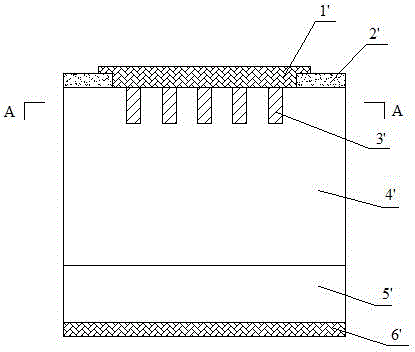
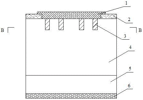
[0041] Step 1, such as Figure 5 As shown, the N-drift layer is epitaxially grown on the N+ silicon carbide substrate: first, the N+ type silicon carbide substrate 5 is cleaned by RCA standard; , Nitrogen ion doping concentration is 5×10 15 cm -3 N - For the epitaxial layer 4, the epitaxial process conditions are as follows: the temperature is 1580° C., the pressure is 100 mbar, the reaction gas is silane and propane, the carrier gas is pure hydrogen, and the impurity source is liquid nitrogen.

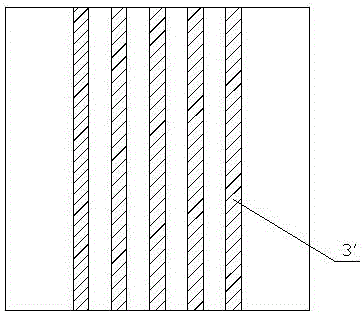
[0042] Step 2, such as Image 6 As shown, a ring-shaped floating-point type P+ implantation region 3 is formed on the N- epitaxial layer: (2.1) Deposit 2 μm of SiO 2 As a barrier layer for Al ion implantation in the P+ implantation area, and form the implantation window of the ring-shaped floating-point P+ implantation area 3 by photolithography and etching; (2.2) Perform aluminum ion implantation three times at a temperature of 400 ° C, and the The doses were 1.33×10 14 cm -2 ...

Embodiment 2

[0047] Step 1, such as Figure 5 As shown, the N-drift layer is epitaxially grown on the N+ silicon carbide substrate: first, the N+ type silicon carbide substrate 5 is cleaned by RCA standard; , nitrogen ion doping concentration is 1×10 15 cm -3 The epitaxy process conditions of the N- epitaxial layer 4 are as follows: the temperature is 1580° C., the pressure is 100 mbar, the reaction gas is silane and propane, the carrier gas is pure hydrogen, and the impurity source is liquid nitrogen.

[0048] Step 2, such as Image 6 As shown, a ring-shaped floating-point type P+ implantation region 3 is formed on the N- epitaxial layer: (2.1) Deposit 2 μm of SiO 2 As a barrier layer for Al ion implantation in the P+ implantation area, the implantation window of the ring-shaped floating-point P+ implantation area 3 is formed by photolithography and etching; (2.2) Perform aluminum ion implantation three times at a temperature of 500 ° C, implant The doses were 1.33×10 14 cm -2 , 8.2...

Embodiment 3

[0053] Step 1, such as Figure 5 As shown, the N-drift layer is epitaxially grown on the N+ silicon carbide substrate: first, the N+ type silicon carbide substrate 5 is cleaned by RCA standard; , nitrogen ion doping concentration is 2×10 15 cm -3 The epitaxy process conditions of the N- epitaxial layer 4 are as follows: the temperature is 1580° C., the pressure is 100 mbar, the reaction gas is silane and propane, the carrier gas is pure hydrogen, and the impurity source is liquid nitrogen.

[0054] Step 2, such as Image 6 As shown, a ring-shaped floating-point type P+ implantation region 3 is formed on the N- epitaxial layer: (2.1) Deposit 2 μm of SiO 2 As a barrier layer for Al ion implantation in the P+ implantation area, the implantation window of the ring-shaped floating-point P+ implantation area 3 is formed by photolithography and etching; (2.2) Perform aluminum ion implantation three times at a temperature of 400 ° C, implant The doses were 1.33×10 14 cm -2 , 8.2...


PUM


Abstract

The invention discloses a Sic annular floating-point type P+ structured junction barrier Schottky diode. The Sic annular floating-point type P+ structured junction barrier Schottky diode comprises a Schottky contact region, a SiO2 isolation medium, an N- epitaxial layer, an N+ substrate region and an ohmic contact region, wherein the N- epitaxial layer is arranged on the N+ substrate region, the Schottky substrate region and the SiO2 isolation medium are arranged on the N- epitaxial layer, the ohmic contact region is arranged under the N+ substrate region, and the Sic annular floating-point type P+ structured junction barrier Schottky diode is characterized in that a plurality of floating-point type P+ injection regions are arranged between the N- epitaxial layer and the Schottky contact region. The Sic annular floating-point type P+ structured junction barrier Schottky diode has the advantages that an annular floating-point type P+ structure is introduced on the basis of a traditional junction barrier Schottky (JBS) device, the Schottky contact area of an active region is expanded, a conduction path is expanded, the positive conduction current of the device is increased, the conduction resistance is reduced, the negative leaked current is not obviously increased, and the problem that the positive conduction resistance and the negative breakdown voltage of the device are restricted with each other is solved.

Description

technical field [0001] The invention relates to the technical field of semiconductor chips, in particular to a SiC ring-shaped floating-point type P+ structure junction barrier Schottky diode and a preparation method thereof. Background technique [0002] Wide bandgap semiconductor materials are the third generation of semiconductor materials developed after the first generation of silicon, germanium and the second generation of gallium arsenide, indium phosphide and other materials. Among the third-generation semiconductor materials, silicon carbide (SiC) and gallium nitride (GaN) are among the best. The silicon carbide material technology is mature, and there are high-quality 4-inch wafers, while the gallium nitride material does not have a gallium nitride substrate, and epitaxy can only rely on other materials. Its thermal conductivity is only a quarter of that of silicon carbide, and p-type doping cannot be achieved. This limits the application of gallium nitride mater...

Claims


Application Information

Patent Timeline
Patent Type & Authority Applications(China)
IPC IPC(8): H01L29/872H01L29/06H01L21/329
CPCH01L29/872H01L29/0615H01L29/6606
Inventor 王成森沈怡东钱清友张超周榕榕黎重林薛治祥颜呈祥
Owner JIANGSU JIEJIE MICROELECTRONICS
Why Eureka
Try Eureka