SERS (Surface Enhanced Raman Spectroscopy) microfluidic chip with enhanced substrate integrated on ITO conductive glass and preparation method for SERS microfluidic chip

A microfluidic chip, conductive glass technology, applied in chemical instruments and methods, laboratory containers, material excitation analysis, etc., to achieve the effects of good morphology consistency, good stability and high sensitivity

Active Publication Date: 2016-07-20
CHONGQING UNIV
View PDF3 Cites 27 Cited by
  • Summary
  • Abstract
  • Description
  • Claims
  • Application Information

AI Technical Summary

Problems solved by technology

[0006] The purpose of the present invention is to provide a composite multi-channel SERS microfluidic chip based on the integrated nano-reinforced substrate on the ITO conductive glass to...

Method used


Image

  • SERS (Surface Enhanced Raman Spectroscopy) microfluidic chip with enhanced substrate integrated on ITO conductive glass and preparation method for SERS microfluidic chip
  • SERS (Surface Enhanced Raman Spectroscopy) microfluidic chip with enhanced substrate integrated on ITO conductive glass and preparation method for SERS microfluidic chip
  • SERS (Surface Enhanced Raman Spectroscopy) microfluidic chip with enhanced substrate integrated on ITO conductive glass and preparation method for SERS microfluidic chip

Examples


Embodiment 1

[0033] This embodiment is the design of a microfluidic SERS chip, and the specific steps are as follows:

[0034] (1) The chip in this example consists of an ITO substrate integrated with a metal nano-SERS substrate and a PDMS cover sheet with multiple parallel channels.

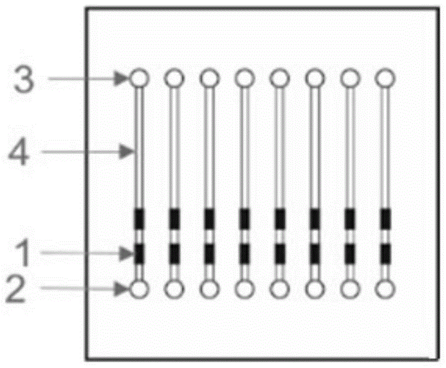
[0035] SERS chip configuration design: In this embodiment, 8 straight channels are designed on a chip of 20 × 20mm, see figure 1 , where 1 is the SERS detection area, and two SERS detection areas are set on each channel, the length of the detection area is 1mm, and the center point is 3mm and 5mm from the exit respectively. 2 and 3 are the positions of the liquid inlet and the liquid outlet, 4 is the microchannel, the length of the microchannel is 12 mm, the width is 200 μm, and the height is 150 μm.

Embodiment 2

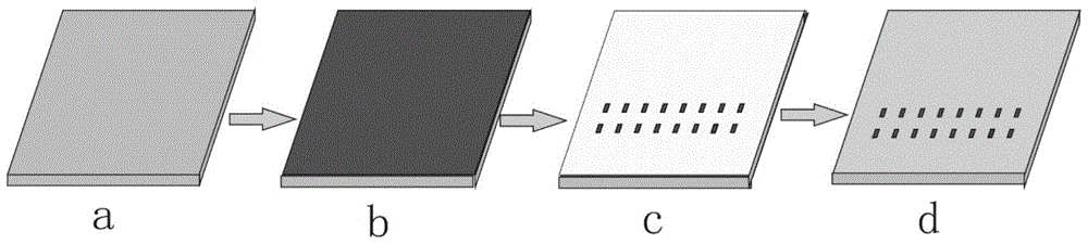
[0036]Example 2 This example is the preparation of a PDMS cover sheet, and the specific steps are as follows: (1) Preparation of SU-8 positive film: According to the set chip configuration, on a silicon wafer, spin-coat SU-8 photoresist, Prepare the chip positive template by UV-soft lithography. The straight channel of the channel protrusion on the template is 12 mm long, 150 μm high, and 200 μm wide.

[0037] (2) Preparation of PDMS cover slip: The cover slip material selected in this example is PDMS, put the SU-8 photoresist film plate into a groove, and pour the prepolymer and the solvent according to the ratio of 1:1. The polydimethylsiloxane (PDMS) elastomer material was vacuum degassed and then placed in an oven at 90°C for 1 hour to heat and cure for 1 hour. The cured PDMS with a microchannel structure and the positive mold were uncovered and separated to obtain the following: Figure 4 b shows a PDMS cover slip with 8 microchannels. The thickness of the cover slip is...

Embodiment 3

[0040] This embodiment is to prepare an ITO conductive glass substrate integrated with a SERS active substrate, comprising the following steps:

[0041] (1) Cleaning of ITO conductive glass: Take a 20mm×20mm ITO conductive glass (resistance less than 10Ω) and use toluene, acetone, ethanol, and ultrapure water to clean it ultrasonically for 15 minutes in order to remove the oil on its surface. Dry and set aside.

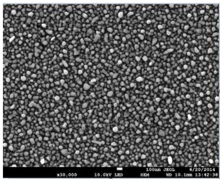
[0042] (2) Electrodeposition integrated nano-silver reinforcement substrate in the SERS detection area: use electrochemical deposition technology to prepare nano-silver SERS substrate on the conductive area of ​​the ITO conductive glass surface, the preparation process is shown in figure 2 .

[0043] First, the three-electrode system of VersaSTAT3 electrochemical workstation was adopted, with platinum electrode as counter electrode, saturated mercury aglycone electrode as auxiliary electrode, and 20mm×20mm ITO conductive glass (10Ωcm-2)) as working electrode. With ...


PUM

PropertyMeasurementUnit
Diameteraaaaaaaaaa
Widthaaaaaaaaaa
Depthaaaaaaaaaa

Abstract

The invention relates to a complex type multichannel SERS (Surface Enhanced Raman Spectroscopy) microfluidic chip based on a nano enhanced substrate integrated on ITO conductive glass and preparation method for the SERS microfluidic chip. According to the SERS microfluidic chip and the preparation method therefor, the ITO conductive glass is used as a substrate surface of an SERS microstructure by making full use the characteristics, i.e., smooth surface and good conductivity of the ITO conductive glass, and the morphology and size of nanoparticles are controlled through controlling the deposition potential and deposition time of the nanoparticles during nucleation and growth by adopting a two-step timed current deposition method, so that a metal-nanostructure SERS substrate with high sensitivity, good stability and uniform distribution can be effectively prepared. Further, the metal-nanostructure SERS substrate is bonded to a PDMS (Polydimethylsiloxane) cover plate containing array type microchannels so as to form and obtain the complex type high-flux SERS microfluidic chip. According to the chip, a plurality of SERS detection areas are manufactured and formed on the same ITO glass, and the nano enhanced substrate is obtained through synchronous electrochemical deposition, so that the morphology consistency is good, and the signal reproducibility is good.

Description

technical field [0001] The invention relates to the technical fields of Surface Enhanced Raman Spectroscopy (Surface Enhanced Raman Spectroscopy, SERS) and microfluidic chip analysis. Background technique [0002] Microfluidic chip analysis methods and technologies have attracted much attention in the analysis and detection of biochemical samples due to their advantages such as small sample volume, flexible structure design, in-situ testing, and easy miniaturization and integration. At present, the detection methods commonly used in microfluidic chips mainly include electrochemical detection, fluorescence detection, and chemiluminescence detection. These methods have high detection sensitivity, but there is a small amount of sample response information, and it is difficult to obtain the detailed structure of biochemical samples. Insufficient information etc. As a non-destructive spectral detection technology, Raman spectroscopy has a fast detection speed and can give inform...

Claims


Application Information

Patent Timeline
IPC IPC(8): B01L3/00G01N21/65
CPCB01L3/502707B01L2200/10G01N21/658
Inventor 徐溢王蓉郑祥权陈李
Owner CHONGQING UNIV
Why Eureka
Try Eureka