Method for preparing organic microchannel plate by employing MEMS technology

A technology of micro-channel plate and micro-channel, which is applied in micro-electro-mechanical system technology and semiconductor fields, can solve the problems of dielectric loss affecting the dynamic uniformity of gain, etc., and achieve the effect of improving gain uniformity, increasing amplitude, and improving characteristic impedance

Inactive Publication Date: 2016-12-07
XI'AN INST OF OPTICS & FINE MECHANICS - CHINESE ACAD OF SCI
View PDF9 Cites 7 Cited by
  • Summary
  • Abstract
  • Description
  • Claims
  • Application Information

AI Technical Summary

Problems solved by technology

At the same time, the dielectric loss will also affect the dynamic uniformity of the gain

Method used


Image

  • Method for preparing organic microchannel plate by employing MEMS technology

Examples


Embodiment Construction

[0042] The present invention is a method for preparing an organic microchannel plate using MEMS technology, which includes the following steps:

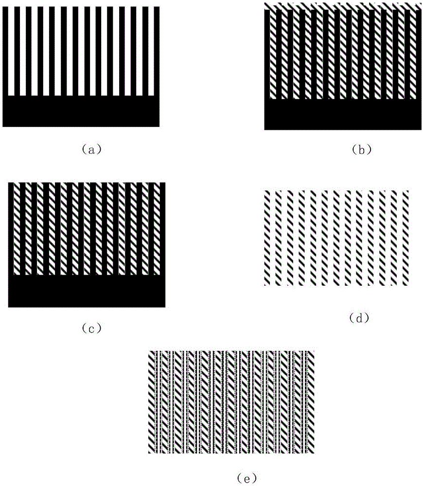
[0043] 1) Using MEMS technology to prepare a silicon-based substrate with a high aspect ratio structure; the high aspect ratio structure is a columnar structure; the preparation adopts dry etching or electrochemical wet etching; the dry etching is specifically: using a mask Membrane material, the microporous structure is etched by reactive ion etching or plasma coupled etching;

[0044] The specific electrochemical wet etching is: the inverted pyramid shape is corroded by KOH, and the treated silicon wafer is electrochemically etched by an anodic oxidation solution composed of HF, tetramethylformamide, hydrochloric acid and an active agent;

[0045] The columnar structure with high aspect ratio prepares a layer of aluminum oxide on the surface of the silicon substrate through the ALD process, which acts as a barrier layer. The aluminum oxid...


PUM


Abstract

The invention provides a method for preparing an organic microchannel plate by employing an MEMS technology. The method comprises the following steps of (1) preparing a silicon-based substrate with a high aspect ratio structure by employing the MEMS technology; (2) depositing organic matters on the silicon-based substrate prepared in the step (1) by employing an ALD or chemical vapor deposition method; (3) removing redundant organic matters on the surface of the silicon-based substrate in a mechanical thinning manner and exposing the upper surface of the substrate; (4) removing the silicon-based substrate in a chemical corrosion manner to form an organic microchannel; and (5) depositing a conductive layer and a secondary electron emission layer in the organic microchannel through an atomic layer deposition process and finally obtaining the organic microchannel plate. The organic microchannel plate prepared by the method has the advantages of a low dielectric constant and a low dielectric loss, and high amplitude and low loss performance of pulse voltage in a framing camera can be ensured, so that the gain strength and the gain uniformity of the framing camera are improved.

Description

Technical field [0001] The invention belongs to the field of microelectromechanical system technology and semiconductor technology, and specifically relates to a method for preparing an organic microchannel plate by adopting a MEMS process. Background technique [0002] Microchannel plate (MCP) is a simple and compact electron multiplying device developed in the late 1960s, which is composed of optical fiber, glass, lead and other materials. It is actually a tiny hollow channel lead glass fiber panel with good secondary emission characteristics and certain conductivity on the inner wall of the channel. [0003] The microchannel plate (MCP) framing tube is the most critical component of the MCP traveling wave strobe X-ray framing camera (MCP-XFC). It is made of the MCP plated with a microstrip line composed of a photocathode and fabricated on a fiber optic panel. The composition of the fluorescent screen. A beam of X-ray or ultraviolet light irradiates the photocathode to generate...

Claims


Application Information

Patent Timeline
Patent Type & Authority Applications(China)
IPC IPC(8): H01J9/233B81C1/00
CPCB81C1/00619H01J9/233
Inventor 曹伟伟朱炳利秦君军白永林王博白晓红缑永胜刘百玉徐鹏
Owner XI'AN INST OF OPTICS & FINE MECHANICS - CHINESE ACAD OF SCI
Why Eureka
Try Eureka