Preparation method of composite transparent electrode using in-situ growth graphene-coated metal film
A graphene-coated, transparent electrode technology, applied in the direction of cable/conductor manufacturing, circuits, electrical components, etc., can solve the problems of affecting the quality of graphene, high substrate requirements, and high corresponding costs, so as to overcome instability Defects, increase light transmittance, overcome the effect of wrinkling
- Summary
- Abstract
- Description
- Claims
- Application Information
AI Technical Summary
Problems solved by technology
Method used
Image
Examples
Embodiment 1
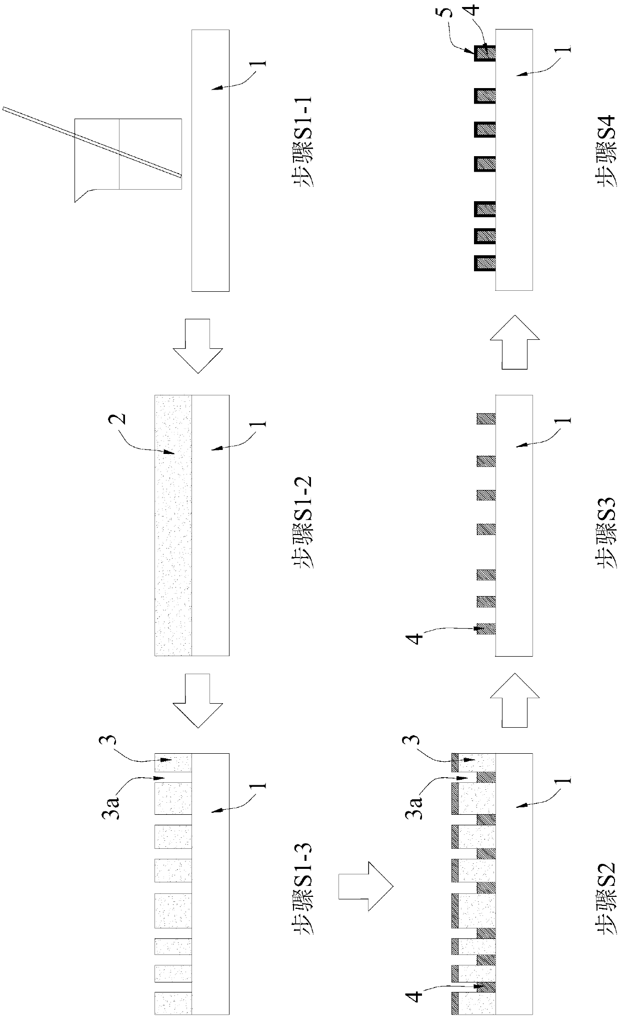
[0041] Such as figure 1 As shown, the method for preparing a composite transparent electrode using in-situ grown graphene-coated metal film according to Embodiment 1 of the present invention includes:
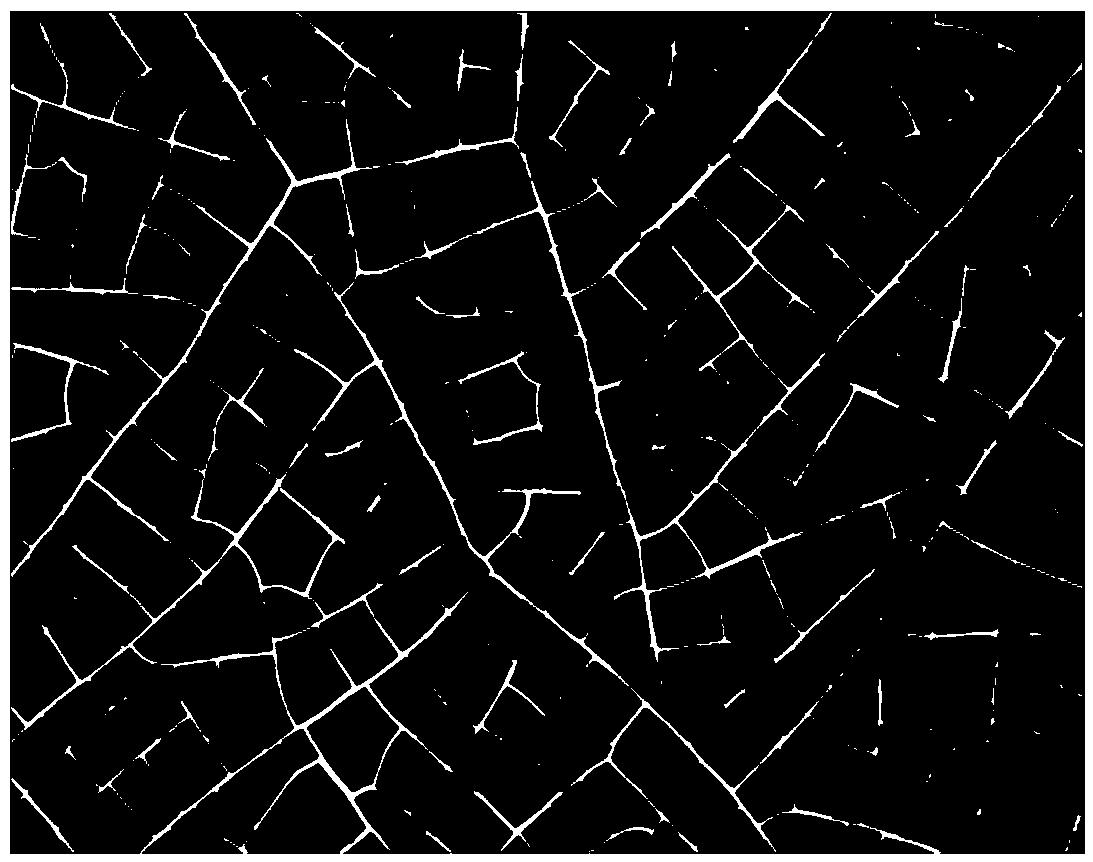
[0042] Step S1, making a crack template: by depositing a layer of organic sol film 2 that is easy to remove on the top surface of the glass substrate 1, and controlling the natural cracking of the organic sol film 2 to form a crack template on the top surface of the glass substrate 1 Split template 3 (see figure 2 ), and the irregular network cracks 3a of the crack template 3 go deep into the top surface of the glass substrate 1 .
[0043] The specific operation steps of the above step S1 are:
[0044] Step S1-1. Mix nail polish CA600 with ethanol solvent at a ratio of 1:2 to make cracking solution. The specific steps are as follows: Take 10ml of CA600 nail polish stock solution in a beaker, then add 20ml of absolute ethanol solution, stir evenly with a glass rod, and place...
Embodiment 2
[0061] Embodiment 2 of the present invention is basically the same as Embodiment 1, and their difference is that in this embodiment 2, the specific operation steps of step S2 are as follows: use high-purity copper as raw material, and use vacuum coating equipment to adopt thermal evaporation in step S2. A copper metal layer with a thickness lower than the thickness of the cracked template 3 is deposited on the top surface of the glass substrate 1 made by S1 to form a mesh metal film 4, wherein the evaporation current when the vacuum coating equipment performs thermal evaporation is 100A, The evaporation voltage is 0.5V, the evaporation time is 20min, and the vacuum degree is 3*10 -4 Torr.
[0062] After testing, the composite transparent electrode made in the second embodiment adopts the thermal evaporation deposition metal film, under vacuum conditions, the evaporator is used to heat the evaporated metal to make it vaporized, and the evaporated particle flow directly shoots t...
Embodiment 3
[0064] Embodiment 3 of the present invention is basically the same as Embodiment 1, and their difference is that in step S2 of Embodiment 3, the power of the vacuum coating equipment when performing magnetron sputtering is 150W, and the temperature in the magnetron chamber is 25°C. The rate of depositing the copper metal layer is 12nm / min, and the thickness of the mesh metal thin film 4 obtained in this step is between 200nm and 400nm.
[0065] After testing, the composite transparent electrode made in this example 3, because the deposition rate of magnetron sputtering is proportional to the power, due to the reduction of the power of magnetron sputtering, the rate of depositing metal is reduced, thus under the same time condition , the thickness of the obtained metal network structure is relatively small, which reduces the overall performance of the composite transparent electrode.
PUM
| Property | Measurement | Unit |
|---|---|---|
| electrical resistivity | aaaaa | aaaaa |
| viscosity | aaaaa | aaaaa |
| thickness | aaaaa | aaaaa |
Abstract
Description
Claims
Application Information


