Manufacturing method of semiconductor device

A manufacturing method and semiconductor technology, applied in the direction of semiconductor devices, semiconductor/solid-state device manufacturing, transistors, etc., can solve the problems of low temperature, impurity activation rate of semiconductor devices is not ideal, etc., to reduce the lifetime of minority carriers, improve the conduction voltage drop, Effect of Reducing Switching Loss

Inactive Publication Date: 2017-03-29
HANGZHOU SILAN INTEGRATED CIRCUIT
View PDF5 Cites 1 Cited by
  • Summary
  • Abstract
  • Description
  • Claims
  • Application Information

AI Technical Summary

Problems solved by technology

However, the inventors found that due to the low temperature of the low-temperature annealing p

Method used


Image

  • Manufacturing method of semiconductor device
  • Manufacturing method of semiconductor device
  • Manufacturing method of semiconductor device

Examples


Embodiment 1

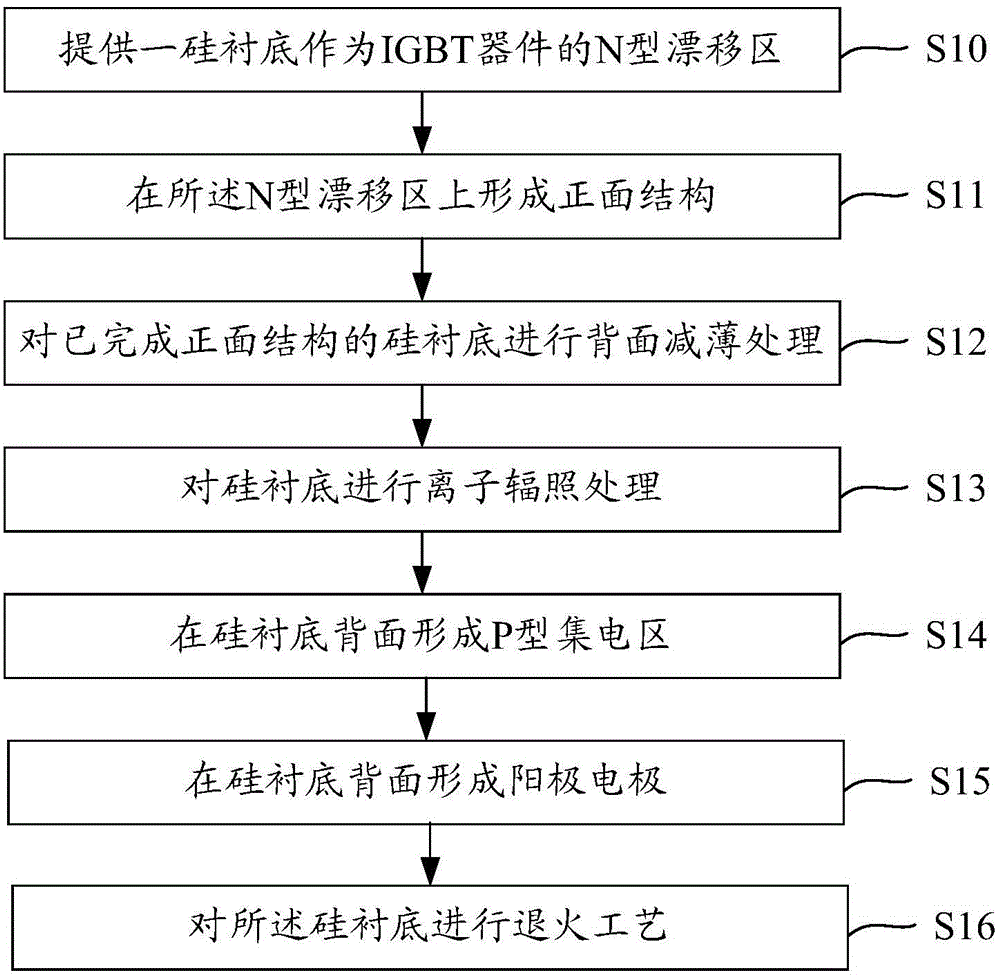
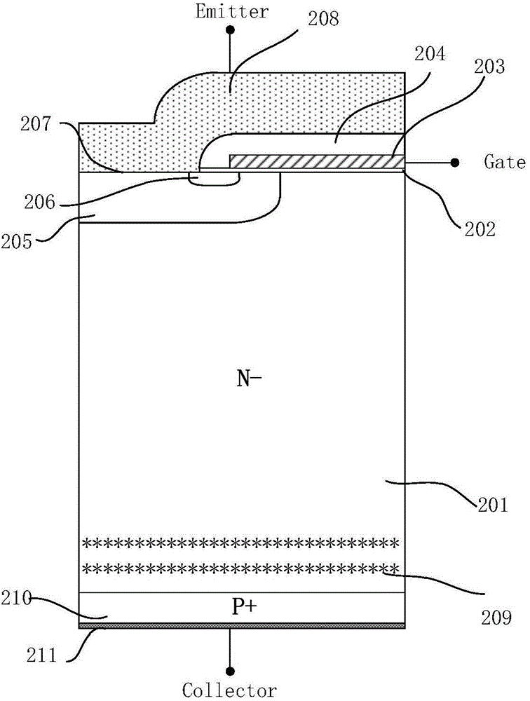
[0035] Take NPT type IGBT device as an example below, combined with attached Figure 1~3 The manufacturing method of the semiconductor device provided by the present invention is described in detail. The IGBT is a composite power device of MOS and BJT, and the NPT IGBT refers to a four-layer structure IGBT device.

[0036] First, perform step S10 to provide a silicon substrate as the N-type drift region 201 of the IGBT device. The silicon substrate can be a CZ wafer (Czochralski monocrystalline silicon wafer) obtained by the Czochralski method, or a pass-through region. The doping concentration of FZ wafers (zone-melting monocrystalline silicon wafers) obtained by the melting method can be freely selected. In this embodiment, the silicon substrate is N-type For the silicon wafer with crystal orientation, the resistivity of the silicon substrate is preferably between 20 and 80 ohm*cm.

[0037] Next, step S11 is performed to form a front structure on the N-type drift region 201. T...

Embodiment 2

[0046] Take NPT type PIN diode as an example, combined Figure 4~5 The manufacturing method of the semiconductor device provided by the present invention is described in detail. The PIN diode refers to a device in which a layer of intrinsic semiconductor is sandwiched between a P-type semiconductor and an N-type semiconductor.

[0047] First, perform step S30 to provide a silicon substrate as the N-type drift region 401 of the PIN diode. The silicon substrate can be a CZ silicon wafer obtained by the Czochralski method or an FZ silicon wafer obtained by the zone melting method. , Its doping concentration can be freely selected. In this embodiment, the silicon substrate is N-type For the silicon wafer with crystal orientation, the resistivity of the silicon substrate is preferably between 20 and 80 ohm*cm.

[0048] Next, step S31 is performed to form a front surface structure on the N-type drift region 201. The front structure includes: a P+ anode region 402 and a cathode electr...


PUM


Abstract

The invention provides a manufacturing method of a semiconductor device. The method comprises the following steps: performing ion irradiation treatment on a back of a silicon substrate to promote an activation rate of anodic impurities of the semiconductor device, improve the breakover voltage drop of the semiconductor device and lower the breakover loss; and forming an extra compound center in the silicon substrate after annealing the silicon substrate through the ion irradiation treatment, thereby reducing the minority carrier lifetime of the semiconductor device and achieving an aim of lowering the switch loss of the semiconductor device. Furthermore, a metal layer is directly deposited on the back of the silicon substrate after injecting the impurity ions into the back of the silicon substrate; and then the annealing process is performed on the silicon substrate, namely, the impurity activation of the semiconductor device and the metal alloy process are integrated, the aims of impurity activation and metal alloying are realized at the same time through the annealing process after the deposition of the metal layer without additionally performing the annealing process after the impurity ion injection; the process step is reduced, and the treatment cost is saved.

Description

Technical field [0001] The invention relates to the field of integrated circuit manufacturing, in particular to a method for manufacturing a semiconductor device. Background technique [0002] Power semiconductor devices are also called power electronic devices, including power diodes, thyristors, VDMOS (vertical double diffused metal oxide semiconductor) field effect transistors, LDMOS (laterally diffused metal oxide semiconductor) field effect transistors, and IGBTs (insulated gate bipolar) Transistor) etc. Among them, IGBT is a composite fully controlled voltage-driven power semiconductor device composed of BJT (bipolar transistor) and FET (field effect transistor). Because it has the advantages of both BJT and FET, that is, high input impedance and low The characteristic of conduction voltage drop, so it has good switching characteristics, and is widely used in fields with high voltage and high current characteristics, such as AC motors, inverters, switching power supplies, ...

Claims


Application Information

Patent Timeline
IPC IPC(8): H01L21/331H01L21/329H01L21/265
CPCH01L29/66333H01L21/26506H01L29/6609
Inventor 顾悦吉王珏杨彦涛黄示
Owner HANGZHOU SILAN INTEGRATED CIRCUIT
Why Eureka
Try Eureka