Manufacture method of high-efficiency cell with front emission junction and backside tunneling oxidation and passivation contact

A technology of tunnel oxidation and manufacturing method, which is applied in the manufacture of circuits, electrical components, final products, etc., can solve the problems that the electrical performance is not greatly improved, achieve easy compatibility, improve open circuit voltage and conversion efficiency, and have strong process feasibility Effect

Inactive Publication Date: 2017-05-31
SHANGHAI SHENZHOU NEW ENERGY DEV
View PDF6 Cites 9 Cited by
  • Summary
  • Abstract
  • Description
  • Claims
  • Application Information

AI Technical Summary

Problems solved by technology

Chinese patent CN102544198A discloses a method for preparing a selective emission crystalline silicon solar cell, including single-step high-concentration doping diffusion, and then printing anti-corrosion paste on the electrode area by printing process, and chemically etching the non-electrode area to achieve light doping The emitter junction, and then remove the anti-corrosion barrier layer, and finally use the conventional solar energy preparation method to make the selective emission crystalline silicon solar cell, but this patent application still uses the back point contact of the N-type crystalline silicon cell, so the electrical performance is not great. improvement

Method used


Image

  • Manufacture method of high-efficiency cell with front emission junction and backside tunneling oxidation and passivation contact

Examples


Embodiment 1

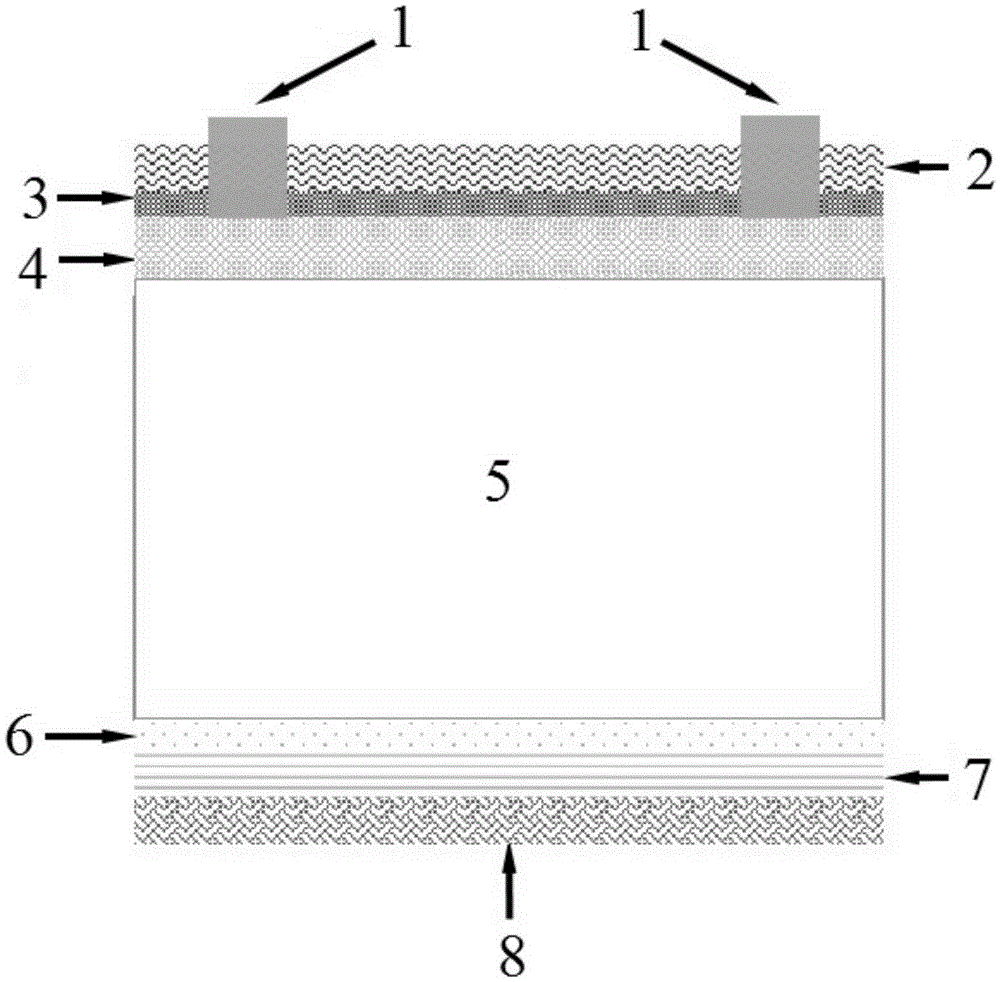
[0023] A method for making a high-efficiency cell with an oxidation passivation contact on the back side of the front emitter junction adopts the following steps:

[0024] (1) Using the silicon chip in KOH alkali solution and H 2 o 2 Remove the damaged layer in the solution, then use tetramethylammonium hydroxide and isopropanol to form a mixed solution to texture the silicon wafer, and form a pyramid texture with 1 μm on both sides;

[0025] (2) In the boron source high-temperature diffusion furnace tube, the temperature is controlled at 850 ° C for 40 minutes, and then the temperature is controlled at 800 ° C to pass oxygen into the junction to form a low surface concentration B-doped P + launch junction;

[0026] (3) Use HF solution to remove borosilicate glass BSG layer, and use HNO 3 Mixed solution with HF for side insulation and back polishing;

[0027] (4) Using wet chemical method to grow an ultra-thin tunnel oxide layer SiO on the back of the silicon wafer 2 , it...

Embodiment 2

[0033] A method for making a high-efficiency cell with an oxidation passivation contact on the back side of the front emitter junction adopts the following steps:

[0034] (1) Using the silicon chip in NaOH alkali solution and H 2 o 2 Remove the damaged layer in the solution, then use tetramethylammonium hydroxide and isopropanol to form a mixed solution to texture the silicon wafer, and form a pyramid texture with 2 μm on both sides;

[0035] (2) In the boron source high-temperature diffusion furnace tube, the temperature is controlled at 900°C for 30 minutes, and then the temperature is controlled at 850°C to pass oxygen into the junction to form a low surface concentration B-doped P + launch junction;

[0036] (3) Use HF solution to remove borosilicate glass BSG layer, and use HNO 3 Mixed solution with HF for side insulation and back polishing;

[0037] (4) Using wet chemical method to grow an ultra-thin tunnel oxide layer SiO on the back of the silicon wafer 2 , its t...

Embodiment 3

[0042] A method for making a high-efficiency cell with an oxidation passivation contact on the back side of the front emitter junction adopts the following steps:

[0043] (1) Using the silicon chip in NaOH alkali solution and H 2 o 2 Remove the damaged layer in the solution, then use tetramethylammonium hydroxide and isopropanol to form a mixed solution to texture the silicon wafer, and form a pyramid texture with 4 μm on both sides;

[0044] (2) In the boron source high-temperature diffusion furnace tube, the temperature is controlled at 1000 ° C for 20 minutes, and then the temperature is controlled at 900 ° C to pass oxygen into the junction to form a low surface concentration B-doped P + launch junction;

[0045] (3) Use HF solution to remove borosilicate glass BSG layer, and use HNO 3 Mixed solution with HF for side insulation and back polishing;

[0046] (4) Using wet chemical method to grow an ultra-thin tunnel oxide layer SiO on the back of the silicon wafer 2 , ...


PUM


Abstract

The invention relates to a manufacture method of a high-efficiency cell with a front emission junction and backside tunneling oxidation and passivation contact. Texturing is carried out after removing a damage layer of a silicon chip, a B-doped P+ emission junction of a low surface concentration is formed, an ultrathin tunneling oxide layer SiO2 and a P-doped polysilicon layer are grown in the back side of the silicon chip after edge insulation and backside polishing, an alumina layer is deposited in the surface of the P+ emission junction, a hydrogenated amorphous silicon nitride passivation antireflection layer is grown in the front side of the silicon chip in a PECVD or magnetron sputtering method, a Ag/Al slurry is printed in the front side of the silicon chip, a full aluminum backfield Al-BSF structure is formed in the back side of the silicon chip, and a drying furnace is used to implement drying. Compared with the prior art, the ultrathin tunneling oxide SiO2 layer (<2nm) and the P-doped silicon layer are used to reduce metal-semiconductor surface combination in the backside greatly, and the manufacture method has the obvious advantage that electric performance parameters can be improved greatly on the basis that the method is compatible with a traditional cell manufacturing technology.

Description

technical field [0001] The invention relates to a method for manufacturing a crystalline silicon cell, in particular to a method for manufacturing a high-efficiency cell with an oxidation passivation contact on the back side of a front emitter junction. Background technique [0002] The difference between front-emitter junction back tunnel oxidation passivation contact cell technology and conventional battery technology is the preparation of the composite structure of back tunnel oxidation passivation layer and doped polysilicon layer. The key point of this method is the ultra-thin tunnel Preparation control of the through-oxide layer and treatment of the interface state with the silicon substrate before preparation. Chinese patent CN102544198A discloses a method for preparing a selective emission crystalline silicon solar cell, including single-step high-concentration doping diffusion, and then printing anti-corrosion paste on the electrode area by printing process, and che...

Claims


Application Information

Patent Timeline
Patent Type & Authority Applications(China)
IPC IPC(8): H01L31/18
CPCH01L31/1804Y02P70/50
Inventor 汪建强钱峥毅郑飞林佳继张忠卫石磊阮忠立
Owner SHANGHAI SHENZHOU NEW ENERGY DEV
Why Eureka
Try Eureka