Pure inorganic perovskite light emitting diode device manufacturing method

A technology of light-emitting diodes and inorganic calcium, which is applied in the fields of organic semiconductor devices, semiconductor/solid-state device manufacturing, electric solid-state devices, etc., can solve the problems of complex process, small selection of hole transport materials, long preparation time, etc., and achieves the difficulty of preparation. Low, improve the flatness and uniformity, the effect of stable performance

Inactive Publication Date: 2017-10-20
SUZHOU UNIV
View PDF5 Cites 29 Cited by
  • Summary
  • Abstract
  • Description
  • Claims
  • Application Information

AI Technical Summary

Problems solved by technology

[0006] Aiming at the existing disadvantages of preparing pure inorganic perovskite light-emitting diode devices, such as complex process, long preparation time, and small selection of hole transport materials, the present invention provides a preparation method of pure inorganic perovskite light-emitting diode devices. The preparation method The process of device preparation is simplified, and the selection of hole transport materials is wide, which makes the device preparation stable and saves steps and costs

Method used


Image

  • Pure inorganic perovskite light emitting diode device manufacturing method
  • Pure inorganic perovskite light emitting diode device manufacturing method
  • Pure inorganic perovskite light emitting diode device manufacturing method

Examples


Embodiment 1

[0030] The formation process of the perovskite layer:

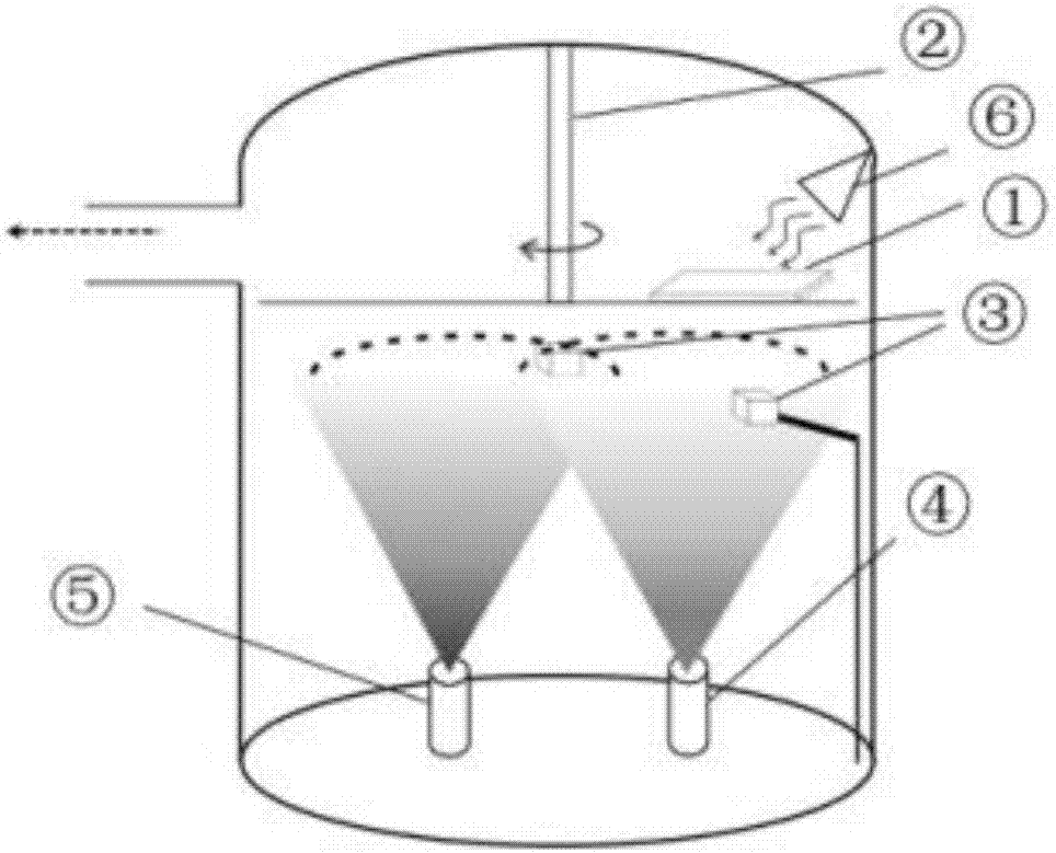
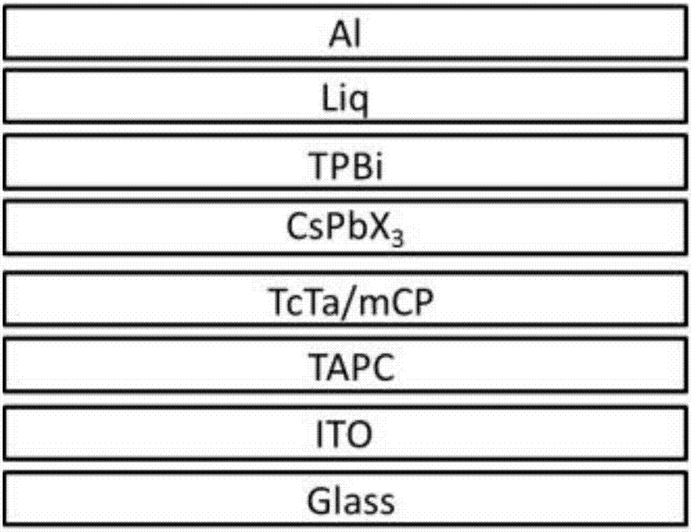
[0031] The perovskite material is placed directly in a grooved handmade tantalum skin boat and heated. The organic small molecule material is placed in the quartz boat, and the quartz boat is placed on the handmade tantalum skin. Precursor material CsPbX 3 It can be heated and sublimated to generate a beam, and the tray for placing ITO ( figure 1 Middle ②) Deposit perovskite molecular layers layer by layer at a speed of 25 rpm to form perovskite crystals. The grain size of perovskite can be controlled by rotation speed and evaporation rate. Here, the rotation speed and evaporation rate were optimized to 25 rpm and 1 Å / s. During the deposition process, the host and guest perovskite materials PbBr 2 , the position of CsBr is controlled to be 180° to achieve the uniform deposition of monoatomic layers to form lattice-dense perovskite layers. When the molar ratio of Pb and Cs precursor materials is 1:1.2, the produced P...

Embodiment 2

[0041] Example 2

[0042] The difference with Example 1 is that the method of dual-source co-evaporation is adopted in step 4, with PbI 2 CsI ​​is the host material, CsI is the guest material, and the molar ratio is 1 to 1.2, forming a perovskite light-emitting layer.

Embodiment 3

[0044] The difference between embodiment 3 and embodiment 1 is that in step 4, the method of dual-source co-evaporation is adopted, and PbCl 2 As the host material, CsCl as the guest material, the molar ratio is 1 to 1.2, forming a perovskite light-emitting layer.

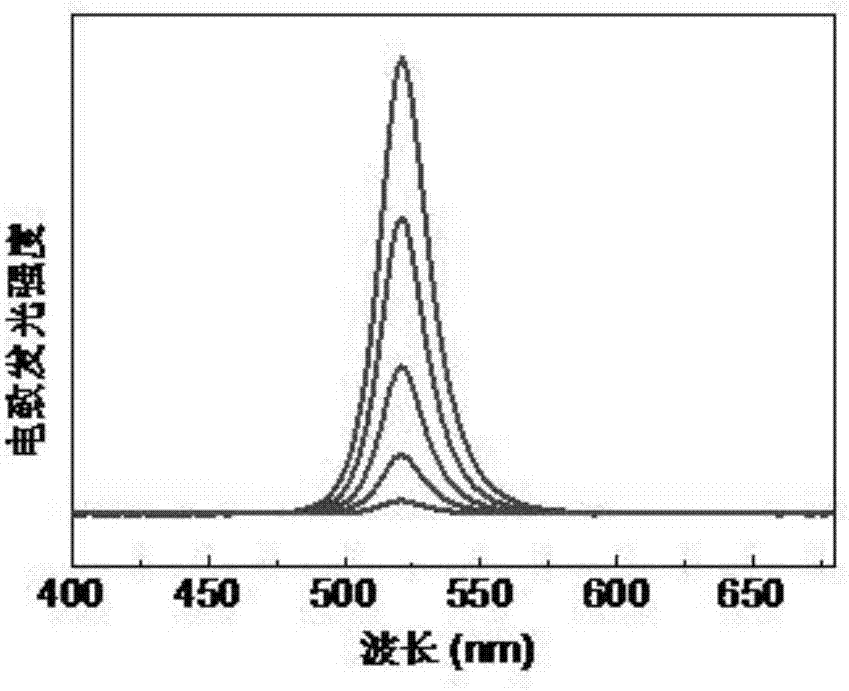
[0045] With the ITO substrate after the 5th step processing in embodiment 1, use the fluorescent spectrogram that the fluorescent spectrometer tests to obtain, from image 3 It can be seen from the figure that the fluorescence peak of the inorganic perovskite layer in Example 1 is at the position of 524 nm, and the half-wave width is 19 nm; Figure 4 It can be seen that the peak positions of the inorganic perovskite layer in Example 1 are at (100), (110), (200), and (202). Place the ITO substrate processed in the fifth step in Example 1 in the vacuum chamber of a photoelectron spectrometer (XPS), and evacuate to 2.0×10 -8 Pa, UV photoelectron spectrum measured with HeI as UV light source (21.2 eV), from Figure...


PUM

PropertyMeasurementUnit
thicknessaaaaaaaaaa
thicknessaaaaaaaaaa
thicknessaaaaaaaaaa

Abstract

The invention provides a pure inorganic perovskite light emitting diode device manufacturing method. The method comprises the following steps: (1) an ITO transparent conductive glass substrate is subjected to standardized cleaning and drying and then pretreatment; (2) the ITO is transferred to a vacuum cavity, and evaporation on a hole injection layer and a transport layer is carried out; (3) a dual source co-evaporation method is adopted, and a pure inorganic CsPbX3 perovskite light emitting layer thin film is formed through evaporation; (4) an infrared thermal radiation device is used to carry out thermal treatment on the CsPbX3 perovskite film; and (5) an electron transport layer, an electron injection layer and a metal cathode are formed through thermal evaporation. The manufacturing process is simple and convenient, the manufacturing difficulty is low, the full vacuum evaporation method is adopted to manufacture the device, the manufacturing is easy, the repeatability is good, and the device performance is stable; and through the dual source co-evaporation manufacturing method, the smoothness and the uniformity of the thin film are improved, replacement of a subject material and an object material is facilitated, the ratio of the two can be changed, and regulation on the position of a light emitting peak is realized.

Description

technical field [0001] The invention belongs to the field of semiconductor devices, in particular to a preparation method of a pure inorganic perovskite light-emitting diode device. Background technique [0002] Perovskite organic light-emitting diodes have attracted great attention from academia and industry due to their excellent chromatographic purity (CIE) and potential for commercial applications. The molecular formula of the all-inorganic perovskite material is CsPbX 3 , where Cs is cesium, Pb is lead, and X is one of iodine (I), chlorine (Cl), and bromine (Br). This inorganic perovskite has a fluorescence quantum yield of more than 90% and a narrow emission peak, which has great prospects and research value in the application of light-emitting diodes. [0003] The currently commonly used methods for preparing light-emitting diode devices based on titanium materials more or less use the solution method to prepare the perovskite active layer or carrier transport layer...

Claims


Application Information

Patent Timeline
Patent Type & Authority Applications(China)
IPC IPC(8): H01L51/56H01L51/50H01L51/54
CPCH10K71/164H10K50/11H10K2102/00H10K71/00
Inventor 廖良生王强胡云王照奎
Owner SUZHOU UNIV
Why Eureka
Try Eureka