
Method for achieving growth of monocrystalline silicon through Czochralski method

A technology for growing single crystal silicon and single crystal silicon ingots, applied in the direction of crystal growth, single crystal growth, single crystal growth, etc., can solve problems such as hindering use and uncontrollable growth of silicon dioxide, so as to reduce the amount of use and reduce leakage. Current, the effect of reducing the content

Inactive Publication Date: 2018-01-19
ZING SEMICON CORP
View PDF10 Cites 1 Cited by
  • Summary
  • Abstract
  • Description
  • Claims
  • Application Information

AI Technical Summary

Problems solved by technology

However, the addition of this barium species needs to be very precise, hindering the use of this method
Furthermore, the growth of silica is almost uncontrollable due to the homogeneous distribution of the crystallization accelerator (barium) on the crucible surface

Method used


Image

  • Method for achieving growth of monocrystalline silicon through Czochralski method
  • Method for achieving growth of monocrystalline silicon through Czochralski method
  • Method for achieving growth of monocrystalline silicon through Czochralski method

Examples


Embodiment 1

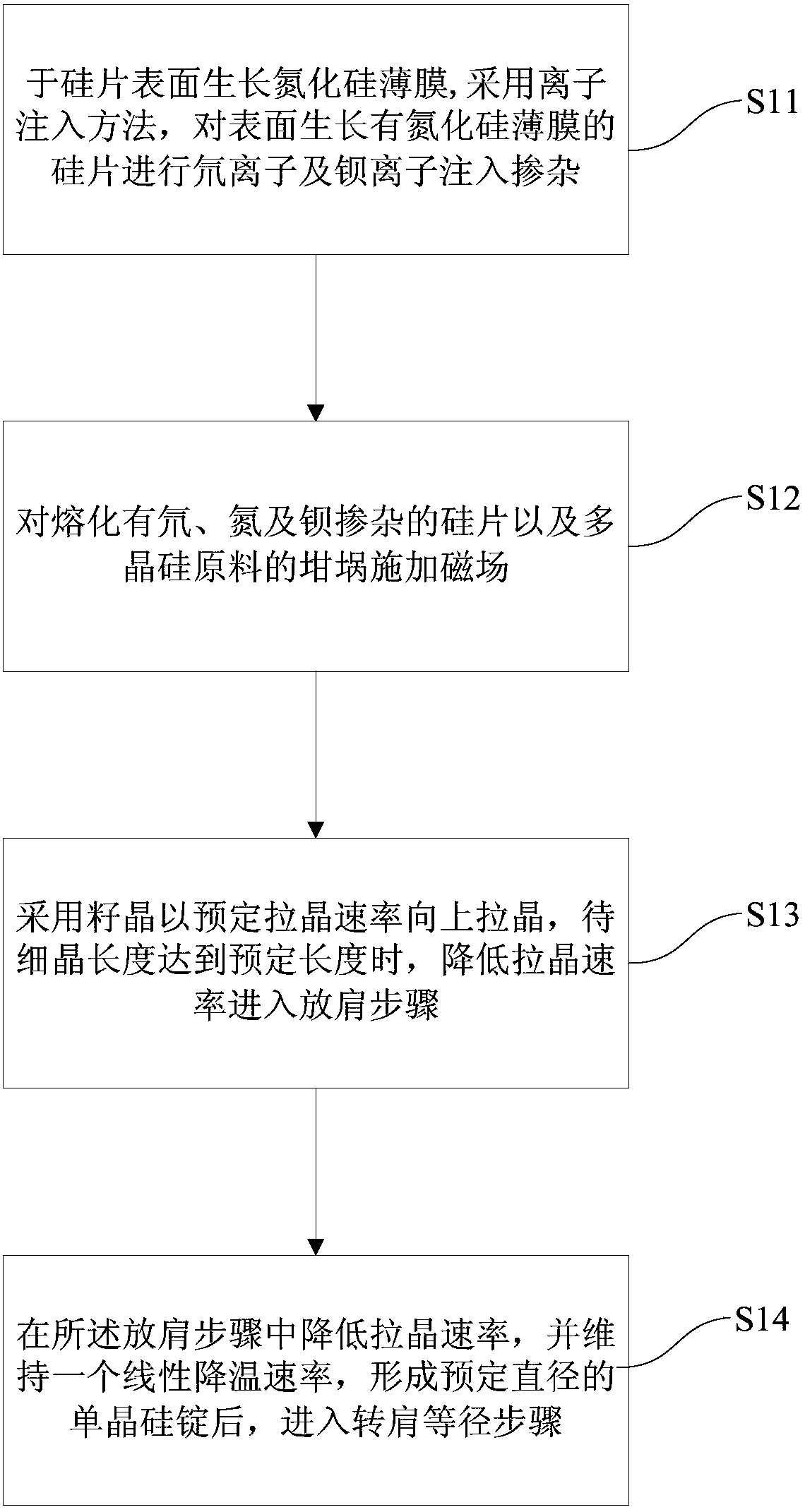
[0036] Such as Figure 2 ~ Figure 3 As shown, the present embodiment provides a method for Czochralski growth of single crystal silicon, the method comprising the following steps:

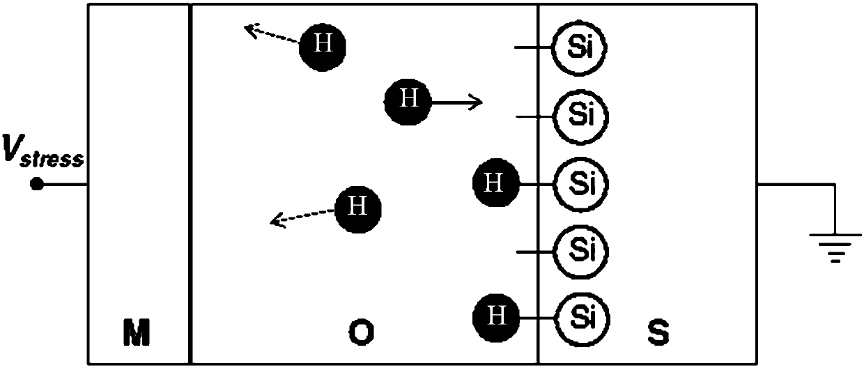
[0037] Such as image 3 As shown, first perform step 1) S11, provide deuterium, nitrogen and barium-doped silicon wafers and polysilicon raw materials, put the silicon wafers and polysilicon raw materials into a crucible for fusion, and put the silicon wafers and polysilicon raw materials into Gas is introduced into the crucible while the gas includes argon.

[0038] In this embodiment, the preparation of the silicon wafer doped with deuterium, nitrogen, and barium includes the steps of: growing a silicon nitride film on the surface of the silicon wafer; Deuterium ion and barium ion implantation doping.

[0039] Wherein, the deuterium ions and barium ions may be implanted into the silicon wafer sequentially, or may be implanted into the silicon wafer at one time at the same time. In this embodi...

Embodiment 2

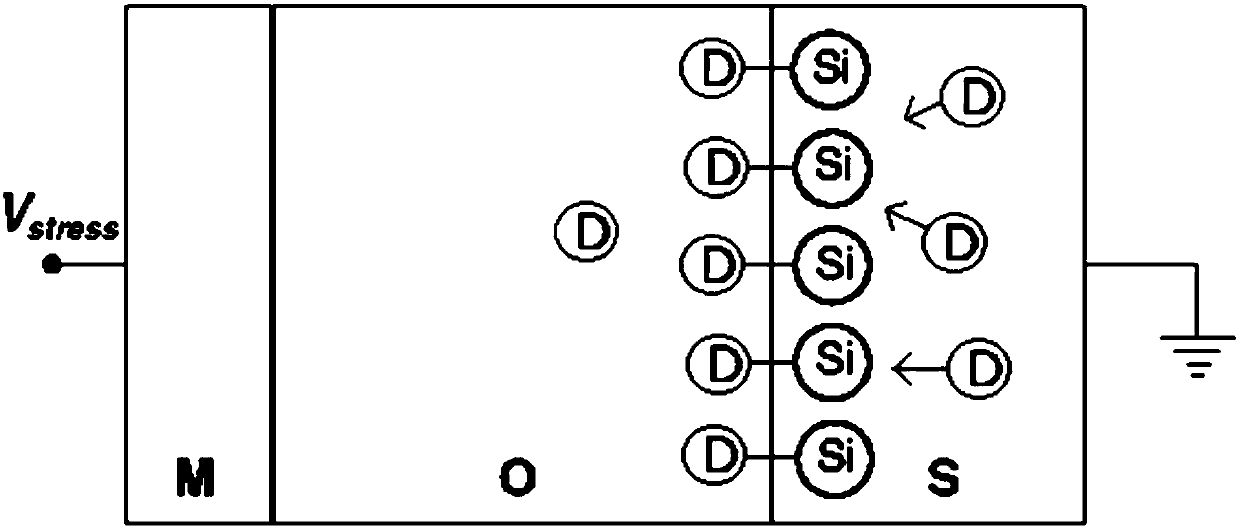
[0053] Such as Figure 4 As shown, this embodiment provides a method for Czochralski growth of single crystal silicon, the basic steps of which are as in embodiment 1, wherein, the difference from embodiment 1 is that in step 1) S21, the deuterium, nitrogen and The preparation steps of the barium-doped silicon chip include: performing ion implantation doping on the silicon chip with deuterium ions, nitrogen ions and barium ions by ion implantation method to form the silicon chip doped with deuterium, nitrogen and barium. In this embodiment, the deuterium ions, nitrogen ions and barium ions may be implanted into the silicon wafer sequentially, or may be implanted into the silicon wafer at the same time. Wherein, the implantation energy range of the deuterium ions is 1keV-1000keV, and the dose is 1E12-1E18ions / cm 2 , the implantation energy range of the nitrogen ions is 1keV-1000keV, and the dose is 1E12-1E18ions / cm 2 , the implantation energy range of the barium ions is 1keV~...


PUM


Abstract

The invention provides a method for achieving the growth of monocrystalline silicon through a Czochralski method. The method comprises the steps of: step (1), providing silicon wafers doped with deuterium, nitrogen and barium ions and a polycrystalline silicon raw material, putting the silicon wafers and the polycrystalline silicon raw material in a crucible for fusion; and step (2), forming the monocrystalline silicon ingot doped with the deuterium and nitrogen ions by using the Czochralski method through the addition of a magnetic field. According to the method for achieving the growth of the monocrystalline silicon through the Czochralski method, the level of impurities in a molten mass and the grown monocrystalline silicon crystal ingot can be reduced, and by performing high-temperature annealing on the nitrogen-doped monocrystalline silicon wafers, COP defects in the surface area of the silicon wafers can be eliminated; by storing the deuterium ions in gaps of the monocrystallinesilicon ingot, the content of impurities of oxygen and carbon can be reduced, and when a device is formed on wafers which grow later, the deuterium ions can combine with vacant bonds at an interface between a gate dielectric layer and a semiconductor to form a stable structure, so that penetration of hot carriers can be avoided; besides, the leakage current is reduced, and the performance and reliability of the device are improved; by doping the silicon wafers with the nitrogen, deuterium and barium ions, the application amount of the doped silicon wafers can be reduced, and the manufacture cost can be reduced.

Description

technical field [0001] The invention belongs to the field of semiconductor manufacturing, in particular to a method for Czochralski growth of monocrystalline silicon. Background technique [0002] The pulling method is widely used to prepare single crystal silicon materials, and quartz crucibles are usually used to carry single crystal silicon melts. The process of the pulling method is to use a seed crystal with a predefined orientation to immerse in the melt, so that the seed crystal and the melt rotate in different directions, and then slowly pull upwards. During the pulling process, the melting The body is gradually pulled up with the seed crystal under the action of surface tension, and cooled and crystallized into a continuous single crystal. During this pulling process, the quartz glass crucible needs to withstand high temperature for several hours, so it must have high mechanical strength, stable chemical properties and thermal stress deformation, so as to ensure th...

Claims


Application Information

Patent Timeline
Patent Type & Authority Applications(China)
IPC IPC(8): C30B15/04C30B29/06
CPCC30B31/22C30B15/04C30B29/06C30B30/04
Inventor 肖德元张汝京
Owner ZING SEMICON CORP
Learn More