A trench gate charge storage type insulated gate bipolar transistor and its manufacturing method
A bipolar transistor and charge storage technology, which is applied in semiconductor/solid-state device manufacturing, circuits, electrical components, etc., can solve the problems of short-circuit safe working area of the device, increase the saturation current density of the device, and reduce the switching speed, etc., to achieve The effect of improving the forward conduction performance and improving the overall performance
- Summary
- Abstract
- Description
- Claims
- Application Information
AI Technical Summary
Problems solved by technology
Method used
Image
Examples
Embodiment 1
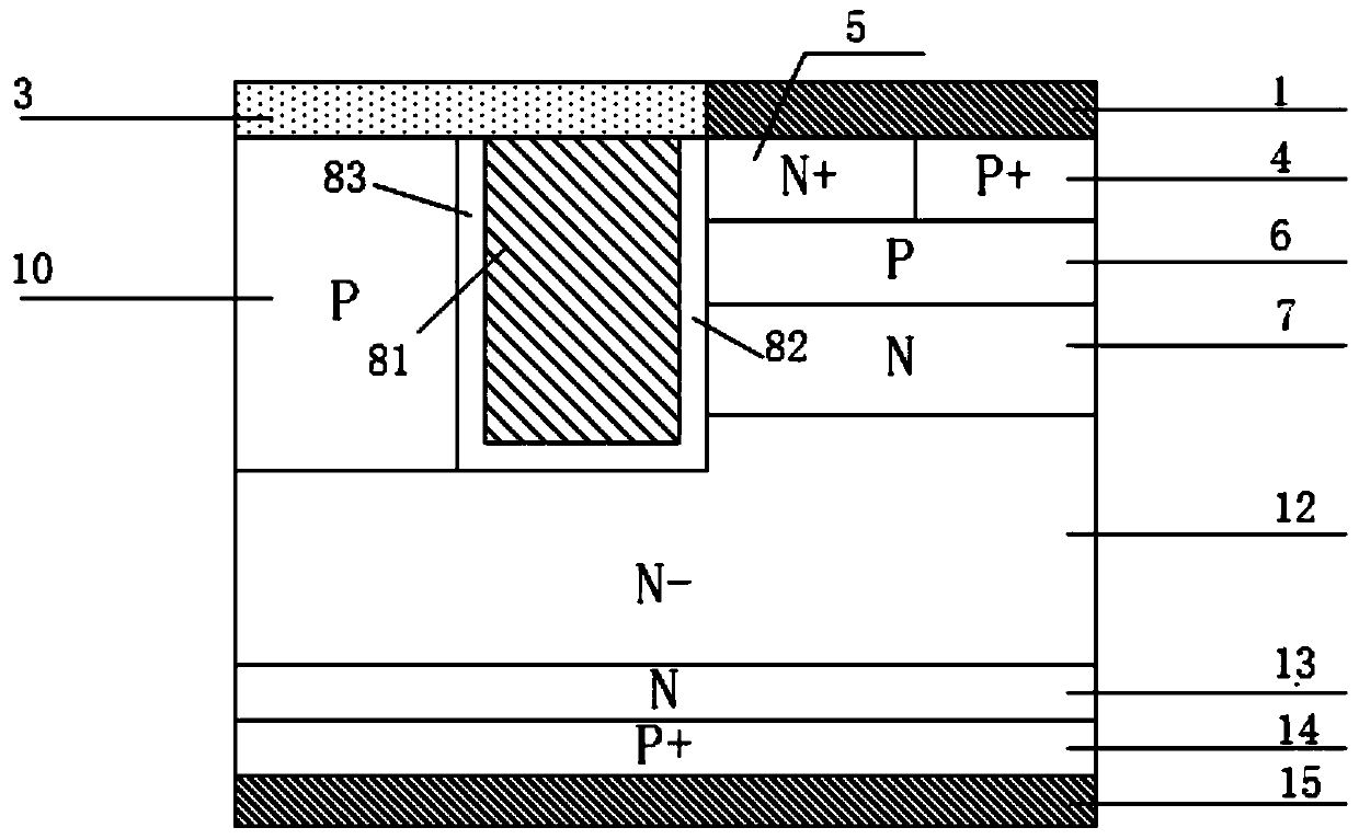
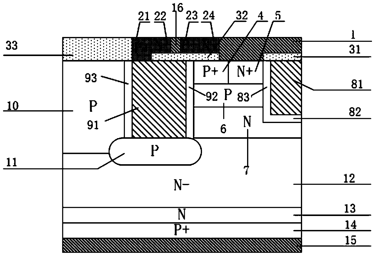
[0066] This example proposes as figure 2 The shown trench gate charge storage type insulated gate bipolar transistor includes: a P-type collector region 14, a collector metal 15 located on the back of the P-type collector region 14, and a The N-type electric field stop layer 13 and the N-type drift region 12 located above the N-type electric field stop layer 13; it is characterized in that: the N-type drift region 12 has a P+ emitter region 4, an N+ emitter region 5, a P-type base region 6, a N-type type charge storage layer 7, trench gate structure, trench emitter structure, P-type body region 10 and P-type layer 11; the middle position of N-type drift region 12 has a trench emitter structure partially penetrating in the vertical direction, so The trench emitter structure includes an emitter electrode 91 and an emitter dielectric layer located on its sidewall;
[0067] The top layer of the N-type drift region 12 on one side of the trench emitter structure has a P+ emitter r...
Embodiment 2
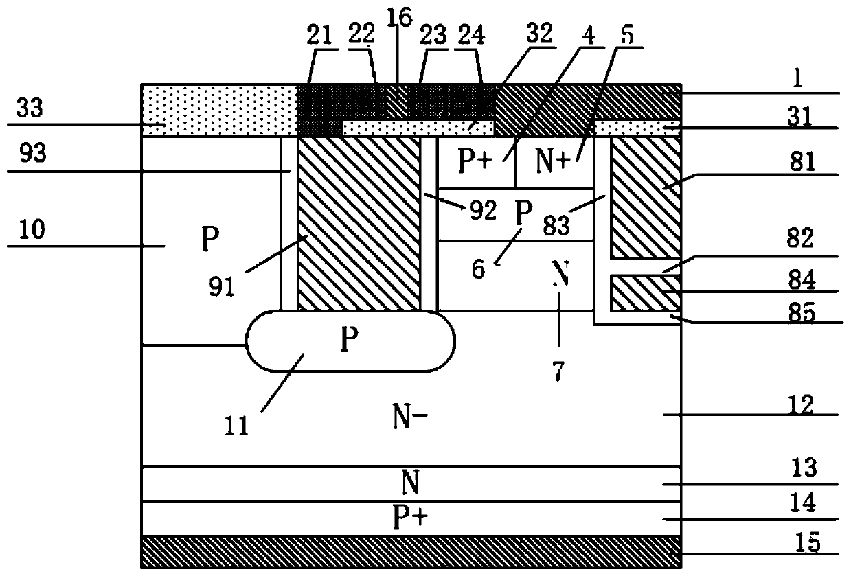
[0071] This example proposes a image 3 In the shown trench gate charge storage type insulated gate bipolar transistor, in this embodiment, in addition to setting a split electrode 84 under the gate electrode 81, which is isolated from it by a gate dielectric layer and has the same potential as the emitter metal 1, and the Except for the split electrode dielectric layer 85 which separates the split electrode 84 from the N-type charge storage layer 7 and the N-type drift region 12 , the other structures are the same as those in Embodiment 1.
[0072] In this embodiment, the shape of the split electrode is not limited. Specifically, the width of the split electrode 84 can be less than or equal to the width of the gate electrode 81; when the width of the split electrode 84 is smaller than the width of the gate electrode 81, it can A step-shaped split electrode dielectric layer is formed at the bottom of the trench, which further reduces the electric field concentration at the bot...
Embodiment 3
[0075] This example proposes a Figure 4 In the shown trench gate charge storage IGBT, the structure of this embodiment is the same as that of Embodiment 1 except that the second P-type layer 1102 is introduced at the bottom of the trench gate structure.
[0076] This embodiment can effectively shield the influence of negative charges in the N-type charge storage layer 7. On the one hand, it is beneficial to reduce the gate capacitance, on the other hand, it improves the concentration of the electric field at the bottom of the trench gate, and improves the breakdown voltage and reliability of the device.
PUM
| Property | Measurement | Unit |
|---|---|---|
| thickness | aaaaa | aaaaa |
Abstract
Description
Claims
Application Information


