Non-contact protection ring single-photon avalanche diode and preparation method thereof
A single-photon avalanche, non-contact technology, applied in the final product manufacturing, sustainable manufacturing/processing, electrical components, etc., can solve the problems of reducing the photon detection efficiency of the device, and it is difficult to trigger an avalanche, so as to facilitate light absorption, The effect of increasing the effective photosensitive area and improving the detection efficiency
- Summary
- Abstract
- Description
- Claims
- Application Information
AI Technical Summary
Problems solved by technology
Method used
Image

Examples
Embodiment 1
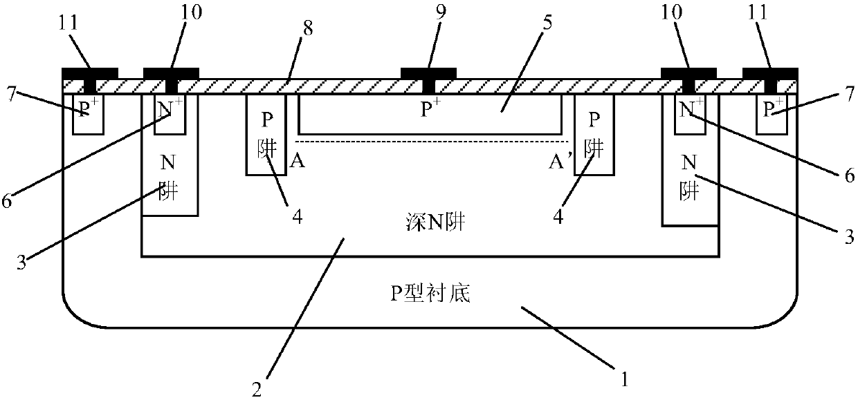
[0039] Embodiments of the present invention propose a single photon avalanche diode detector structure that can effectively suppress edge breakdown and is compatible with standard CMOS processes, see figure 1 , see the description below:
[0040] The detector is mainly composed of P + / Deep N well composed of a photosensitive PN junction and a ring-shaped P well guard ring. The two are separated by a certain distance, and the P well is used to form a guard ring around the photosensitive PN junction to suppress edge breakdown and improve device reliability and detection performance. .
[0041] When the device is working, the P-well guard ring acts as a voltage divider to suppress the increase of the electric field at the edge of the photosensitive area, thereby solving the problem of edge breakdown. In addition, the detector can also increase the effective photosensitive area and increase the detection efficiency.
[0042] In addition, due to the lower doping concentration o...
Embodiment 2
[0044] The embodiment of the present invention also provides a method for manufacturing a non-contact guard ring single photon avalanche diode, comprising the following steps:
[0045] 1) Using standard CMOS processes such as oxidation, photolithography, ion implantation, and annealing to form a lightly doped deep N well on a P-type lightly doped silicon substrate to achieve electrical isolation from other electronic devices and avoid their mutual influence;
[0046]2) Prepare a moderately doped N-type well region in the above-mentioned deep N well region, surround the deep N well region, and then regenerate a thin layer of silicon dioxide;
[0047] 3) Prepare a moderately doped P-type well region in the deep N well as a guard ring for the device;
[0048] 4) A P-type heavily doped region is prepared in the center of the deep N well, which together with the deep N well forms a P + / Deep N well photosensitive PN junction;
[0049] Wherein, the P-type heavily doped region is a...
Embodiment 3
[0057] Attached below Figure 1-4 The scheme in embodiment 1 and 2 is further introduced, see the following description for details:
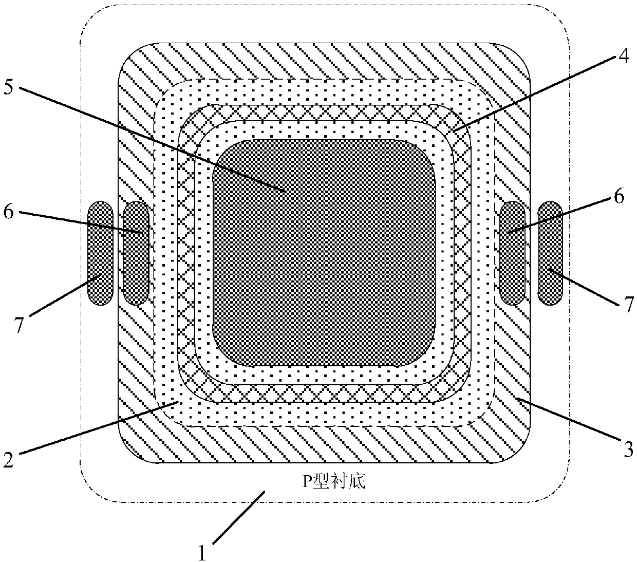
[0058] figure 1 with figure 2 are the cross-section and top view of the detector respectively, for the convenience of explanation, figure 2 The oxide layer 8 and the metal electrodes 9, 10, 11 are not shown.
[0059] In the illustration, 1 is the substrate. The material of the substrate 1 is a P-type lightly doped silicon wafer, which serves as the supporting part of the designed single photon avalanche diode.
[0060] In the figure, 2 is a lightly doped deep N well. On the one hand, the deep N well 2 is used as a component of the photosensitive PN junction, and on the other hand, it is also used to realize the mutual isolation of the detector and other electronic devices.
[0061] In the illustration, 3 is the N well region, and the N well adopts a medium doping concentration and surrounds the deep N well.
[0062] In the illustration,...
PUM
| Property | Measurement | Unit |
|---|---|---|
| Doping concentration | aaaaa | aaaaa |
Abstract
Description
Claims
Application Information
 - Generate Ideas
- Intellectual Property
- Life Sciences
- Materials
- Tech Scout
- Unparalleled Data Quality
- Higher Quality Content
- 60% Fewer Hallucinations
Browse by: Latest US Patents, China's latest patents, Technical Efficacy Thesaurus, Application Domain, Technology Topic, Popular Technical Reports.
© 2025 PatSnap. All rights reserved.Legal|Privacy policy|Modern Slavery Act Transparency Statement|Sitemap|About US| Contact US: help@patsnap.com