Manufacturing method for ultraviolet LED chip
A technology of LED chips and manufacturing methods, which is applied in the direction of electrical components, circuits, semiconductor devices, etc., and can solve problems such as strong absorption loss, adhesion problems, and damage to n-type ohmic contacts
- Summary
- Abstract
- Description
- Claims
- Application Information
AI Technical Summary
Problems solved by technology
Method used
Image

Examples
Embodiment 1
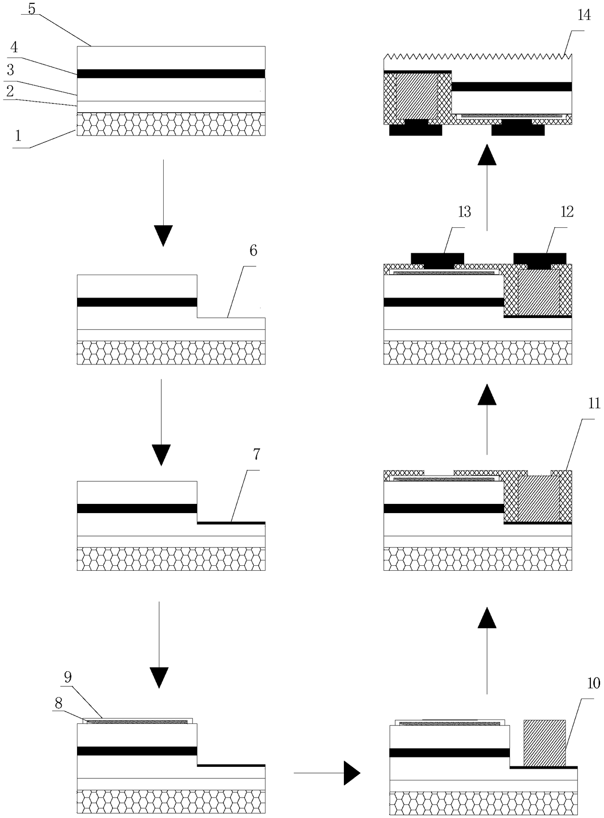
[0060] The present embodiment provides a method for fabricating an ultraviolet LED chip, which includes the following steps:
[0061] S1: sequentially epitaxially grow the u-GaN layer 2, the n-AlGaN layer 3, the multiple quantum well layer 4 and the p-AlGaN layer 5 on the sapphire substrate 1;
[0062] S2: remove the p-AlGaN layer 5, quantum well layer 4 and part of the n-AlGaN layer 3 in a part of the region by photolithography and dry etching, exposing the surface 6 of the n-AlGaN layer to form an n-contact hole;
[0063] S3: A growth barrier layer is grown, and the growth barrier layer on the n-contact hole is etched by photolithography to expose the surface 6 of the n-AlGaN layer;
[0064] Wherein, the growth barrier layer is selected from one or more of a silicon oxide barrier layer, a silicon nitride barrier layer and a silicon oxynitride barrier layer, and the method for growing the barrier layer is one of ALD, PECVD, LPCVD, and magnetron sputtering or more.
[0065] ...
Embodiment 2
[0081] S1: sequentially epitaxially grow the u-GaN layer 2, the n-AlGaN layer 3, the multiple quantum well layer 4 and the p-AlGaN layer 5 on the SiC substrate;
[0082] S2: Remove the p-AlGaN layer 5, quantum wells and part of the n-AlGaN in a part of the region by photolithography and dry etching, exposing the surface 6 of the n-AlGaN layer, and forming an n-contact hole;
[0083] S3: A growth barrier layer is grown, and the growth barrier layer on the n-contact hole is etched by photolithography to expose the surface 6 of the n-AlGaN layer;
[0084]Wherein, the growth barrier layer is selected from one or more of silicon oxide barrier layer, silicon nitride barrier layer and silicon oxynitride barrier layer, and the method for preparing the growth barrier layer is one of ALD, PECVD, LPCVD, and magnetron sputtering. one or more.
[0085] S4: On the surface 6 of the n-AlGaN layer, a thin layer of highly doped n-GaN7 is grown by the MOCVD method, and the growth barrier layer ...
Embodiment 3
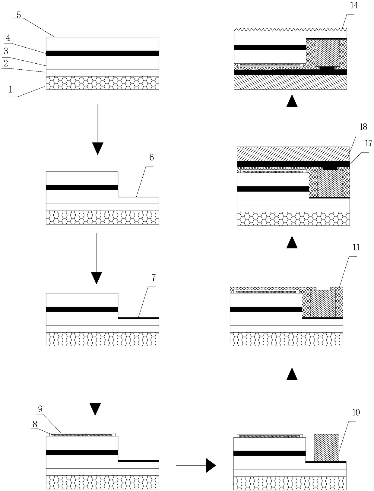
[0103] This embodiment provides a method for fabricating an ultraviolet LED chip. The difference between this fabrication method and the fabrication method provided in Embodiment 1 is that in this embodiment:
[0104] In step S1, an AlN substrate is used as the growth substrate 1, and the u-AlGaN layer 2, the n-AlGaN layer 3, the multiple quantum well layer 4 and the p-AlGaN layer 5 are epitaxially grown on the AlN substrate in sequence;
[0105] In step S4, the MOCVD method is used to grow the n-InGaN layer 7, the n-InGaN thickness is 30 nm, the growth temperature is 950°C, and the doping concentration is 5.0×10 18 cm -3
[0106] In step S5, the annealing condition of the p-type ohmic contact metal is annealing at a temperature of 550°C for 240s;
[0107] In step S7, the annealing condition of the n-type ohmic contact metal is rapid annealing at 260°C for 120s;
[0108] In step S814, the AlN substrate is removed by a laser lift-off method, and the surface of the u-AlGaN la...
PUM
 Abstract
Description
Claims
Application Information
 - R&D Engineer
- R&D Manager
- IP Professional
- Industry Leading Data Capabilities
- Powerful AI technology
- Patent DNA Extraction
Browse by: Latest US Patents, China's latest patents, Technical Efficacy Thesaurus, Application Domain, Technology Topic.
© 2024 PatSnap. All rights reserved.Legal|Privacy policy|Modern Slavery Act Transparency Statement|Sitemap