An aluminum nitride film growing method and application thereof

A technology of aluminum nitride film and growth method, applied in electrical components, nanotechnology, circuits, etc., can solve the problems of low lattice mismatch, line defects, dislocations, cracks, etc., and achieve the suppression of surface cracks. The method is simple and easy OK, high crystal quality results

Active Publication Date: 2018-09-14
MAANSHAN JASON SEMICON CO LTD
View PDF5 Cites 5 Cited by
  • Summary
  • Abstract
  • Description
  • Claims
  • Application Information

AI Technical Summary

Problems solved by technology

Generally, the temperature of high-temperature equipment needs to exceed 1200°C; (2) The lattice mismatch between AlN and the substrate is low, which will easily cause huge internal stress during the growth process of the AlN film, and the stress release will eventually cause Severe cracks are generated on the surface of the AlN film; (3) In order to reduce or eliminate surface cracks, reducing the thickness is one direction, but the reduction in thickness will deteriorate the crystal quality of the AlN film, so that it cannot meet the needs of device preparation; (4) AlN During the growth process of the film, defects such as line defects and dislocations will appear as the thickness increases; (5) The high crystal quality of the AlN film and the integrity of the AlN film without cracks are two contradictory technical problems. At present, in order to obtain High-quality AlN films need to sacrifice surface properties to a certain extent, and in order to obtain excellent surface properties, the crystal quality of AlN films will inevitably decrease

Method used


Image

  • An aluminum nitride film growing method and application thereof
  • An aluminum nitride film growing method and application thereof
  • An aluminum nitride film growing method and application thereof

Examples


Embodiment 1

[0065] The growth method of aluminum nitride film of the present invention comprises the following steps:

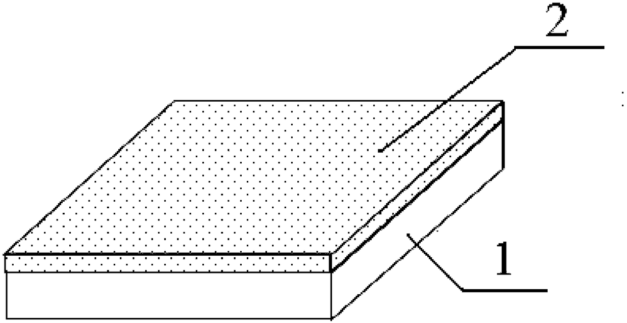
[0066] 1) Take a 2-inch sapphire substrate, raise the temperature of the reaction chamber of the metal-organic chemical vapor deposition (MOCVD) equipment to 1200°C, control the pressure of the reaction chamber at 100mbar, and feed trimethylaluminum at 300ml / min and 10000mL / min Ammonia gas was introduced to react, and after 30 minutes, a first aluminum nitride layer with a thickness of 500 nm was formed on the substrate layer.

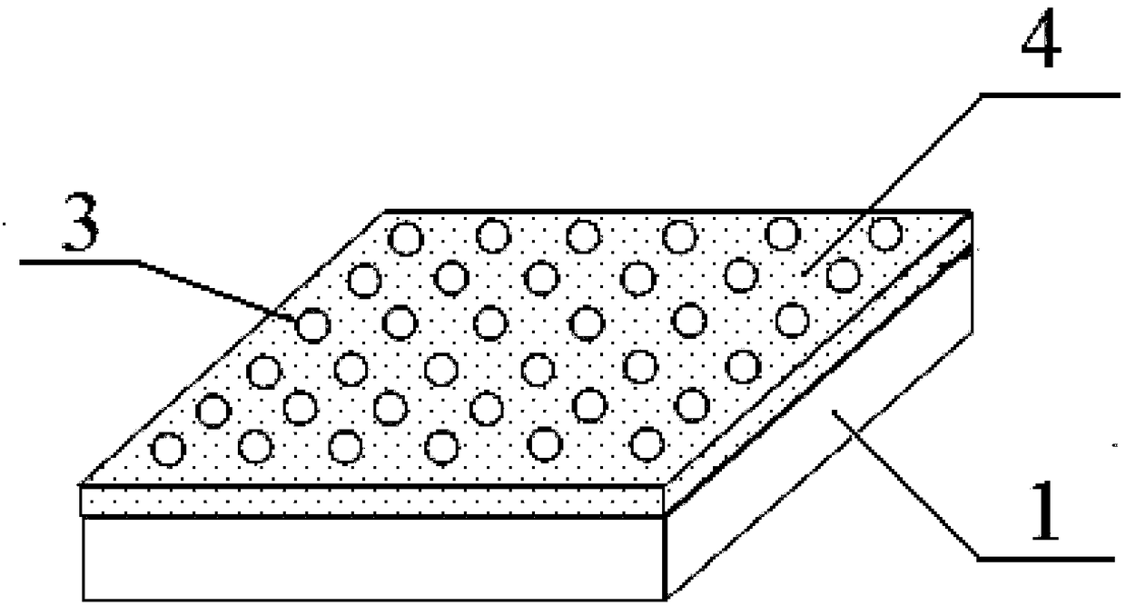
[0067] 2) Take out the substrate layer with the first aluminum nitride layer from the reaction chamber, and etch the nano-scale cylinder depressions on the first aluminum nitride layer to form the aluminum nitride layer with column depressions, wherein the cross-section of the cylinder depressions The diameter of the circle is 200nm, the depth of the cylinder is 300nm, and the distance between the depressions of the cylinders is 500nm;

[0068] ...

Embodiment 2

[0074] The growth method of aluminum nitride film of the present invention comprises the following steps:

[0075] 1) Take a 4-inch sapphire substrate, raise the temperature of the reaction chamber of the metal-organic chemical vapor deposition (MOCVD) equipment to 1200°C, control the pressure of the reaction chamber at 100mbar, and feed trimethylaluminum at 300ml / min and 10000mL / min Ammonia gas was introduced to react, and after 45 minutes, a first aluminum nitride layer with a thickness of 7500 nm was formed on the substrate layer.

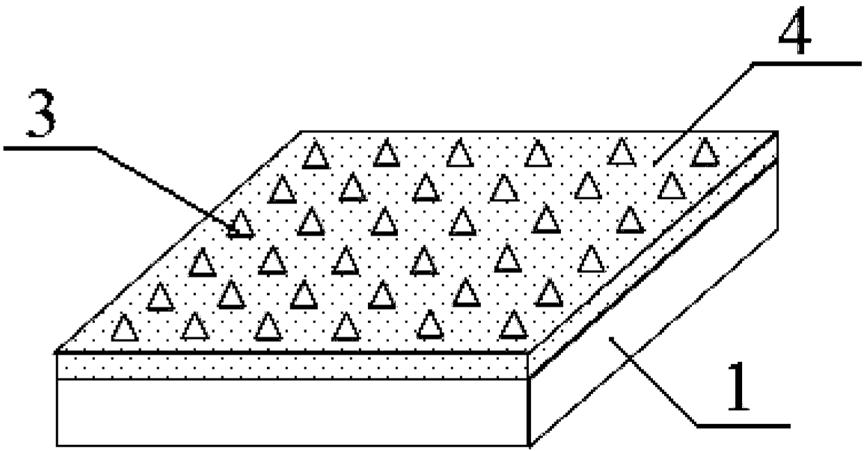
[0076] 2) Take out the substrate layer with the first aluminum nitride layer from the reaction chamber, etch the nano-scale regular triangular prism depressions on the first aluminum nitride layer to form a columnar depression aluminum nitride layer, wherein the regular triangular prism depressions The side length of the cross-sectional triangle is 300nm, the depth of the regular triangular prism is 500nm, and the distance between the regular tr...

Embodiment 3

[0083] The growth method of aluminum nitride film of the present invention comprises the following steps:

[0084] 1) Take a 2-inch sapphire substrate, raise the temperature of the reaction chamber of the metal-organic chemical vapor deposition (MOCVD) equipment to 1200°C, control the pressure of the reaction chamber at 100mbar, and feed trimethylaluminum at 300ml / min and 10000mL / min Ammonia gas was introduced to react, and after 45 minutes, a first aluminum nitride layer with a thickness of 750 nm was formed on the substrate layer.

[0085] 2) Take out the substrate layer with the first aluminum nitride layer from the reaction chamber, etch the nano-scale regular hexagonal prism depression on the first aluminum nitride layer to form a columnar depression aluminum nitride layer, wherein the regular hexagonal prism depression The side length of the regular hexagon in the cross section is 100nm, the depth of the regular hexagonal prism is 300nm, and the distance between the regu...


PUM

PropertyMeasurementUnit
thicknessaaaaaaaaaa
thicknessaaaaaaaaaa
thicknessaaaaaaaaaa

Abstract

The invention provides an aluminum nitride film growing method and application thereof. The growing method comprises the steps of: 1) injecting trimethylaluminum and ammonia gas and growing a first aluminum nitride layer on a substrate; 2) performing nanoscale column body etching processing on the first aluminum nitride layer to obtain a column body recess aluminum nitride layer which has a plurality of nanoscale column body recesses; 3) controlling the temperature and the pressure of a reaction chamber and injecting trimethylaluminum and ammonia gas to grow a second aluminum nitride layer onthe column body recess aluminum nitride layer; 4) controlling the temperature and the pressure of the reaction chamber and injecting trimethylaluminum and ammonia gas to grow a third aluminum nitridelayer on the second aluminum nitride layer. The Mole-flow ratio of ammonia gas to trimethylaluminum in the step 3) is less than that in the step 4); the aluminum nitride film is the integration of thefirst aluminum nitride layer, the second aluminum nitride layer and the third aluminum nitride layer. The AlN thin film crystalline quality is remarkably improved.

Description

technical field [0001] The invention relates to a growth method and application of an aluminum nitride film, belonging to the technical field of light emitting diodes. Background technique [0002] Aluminum nitride (AlN) belongs to the third-generation wide bandgap semiconductor material, which has the advantages of high bandgap width, high breakdown electric field, high thermal conductivity, high electron saturation rate and high radiation resistance. AlN crystal has a stable hexagonal wurtzite structure, the lattice constant AlN has the largest direct band gap of about 6.2eV among III-V non-semiconductor materials, and is an important blue and ultraviolet luminescent material. It has high thermal conductivity, high resistivity, strong breakdown field, and small dielectric coefficient. It is an excellent electronic material for high-temperature, high-frequency and high-power devices. Moreover, AlN oriented along the c-axis has very good piezoelectric properties and high-...

Claims


Application Information

Patent Timeline
Patent Type & Authority Applications(China)
IPC IPC(8): H01L33/00H01L33/12B82Y40/00
CPCB82Y40/00H01L33/007H01L33/12
Inventor 黄小辉梁旭东郑远志
Owner MAANSHAN JASON SEMICON CO LTD
Why Eureka
Try Eureka