Boron nitride material and method of preparation thereof

A technology of boron nitride and amine borane, which is applied in the field of boron nitride materials and its preparation, can solve the problems of film deposition, lack of catalytic activity, epitaxial relationship growth mechanism, etc.

Active Publication Date: 2019-01-11
NANYANG TECH UNIV
View PDF2 Cites 7 Cited by
  • Summary
  • Abstract
  • Description
  • Claims
  • Application Information

AI Technical Summary

Problems solved by technology

However, atomically thin, highly crystalline films cannot be deposited onto Si or other dielectric s

Method used


Image

  • Boron nitride material and method of preparation thereof
  • Boron nitride material and method of preparation thereof
  • Boron nitride material and method of preparation thereof

Examples


example 1

[0148] Example 1: Synthesis of h-BN and h-BCN membranes (Example 1)

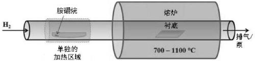
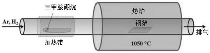
[0149] Copper (Cu) foil (Alfa Asear, product number 13382, 25 micron thick) was used as a growth substrate for the h-BN and h-BCN films. Before growth, the Cu foil was first dipped in dilute nitric acid for a few seconds, and then washed with deionized water to remove the coating on the Cu surface. Then constant Ar / H at 200:20sccm 2 Load the Cu foil into a 1 inch quartz tube by flow down. The furnace was ramped up to 1050°C over 40 minutes and held constant for an additional 30 minutes to anneal the Cu and remove surface oxides.

[0150] After annealing, 10 mg of trimethylamine borane complex (Alfa Asear, Product No. L14994, 97%) placed in a ceramic boat placed outside the heating zone was heated at a specific temperature to start film growth. The growth time for monolayer h-BN single-crystal domains to become continuous films ranged from 5 to 20 min, while for h-BCN films, full coverage films were obta...

example 2

[0151] Example 2: Transfer process (embodiment 1)

[0152] Film transfer to SiO using an electrochemical delayering process 2 / Si and quartz substrates. First, the h-BN or h-BCN film grown on Cu was spin-coated with polymethyl methacrylate (PMMA) at 3000 rpm for 30 s. 1M NaOH was used as electrolyte. Pt foil was used as anode and the spin-coated sample was used as cathode. A constant voltage of 5 V was applied until the PMMA-coated sample was completely separated from Cu.

[0153] The samples were then washed several times in deionized water and transferred to the desired substrate. Bake the transferred samples at 50 °C until they are completely dry. Finally, PMMA was removed by immersing the samples in acetone for several hours.

example 3

[0154] Example 3: Characterization (Example 1)

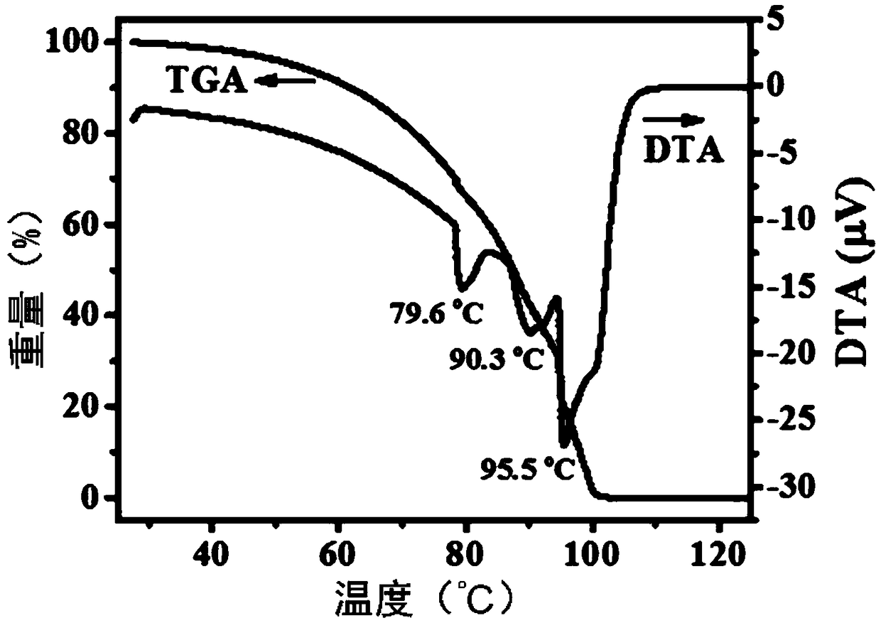
[0155] The thermal decomposition curve of TMAB was determined by thermogravimetric analysis (TGA, Shimadzu DTG-60H thermal analyzer). TGA measurements were performed in a constant nitrogen flow (100 mL / min) and heated from 25°C to 125°C at a ramp rate of 2°C / min.

[0156] Scanning electron microscopy (SEM, LEO1550Gemini) images were taken directly on h-BN and h-BCN films grown on Cu substrates.

[0157] Atomic force microscopy (AFM, Cypher scanning probe microscopy) detection using tapping mode to measure transfer to SiO 2 / Thicknesses of h-BN and h-BCN films on Si substrates.

[0158] Raman spectroscopic detection with a laser excitation wavelength of 532 nm (Witec) was performed at room temperature to measure the transfer to SiO 2 / Crystal structure of films on Si substrates.

[0159] at 4000- 1 -400cm- 1 Fourier-transform infrared spectroscopy (FT-IR, IRPrestige-21 spectrometer) detection was performed using h-BN films ...


PUM


Abstract

A method of preparing a boron nitride material, such as boron nitride (BN) or boron carbonitride (BCN), is provided. The method may include providing a substrate, and sublimating an amine borane complex onto the substrate to obtain the boron nitride material. The amine borane complex may include, but is not limited to, borazine, amino borane, trimethylamine borane and triethylamine borane. In addition, the temperature at which the sublimating is carried out may be varied to control composition of the boron nitride material formed. In addition, various morphologies can be obtained by using thepresent method, namely films, nanotubes and porous foam.

Description

[0001] Cross References to Related Applications [0002] This application claims priority from Singapore Patent Application No. 10201600155R filed on 8 January 2016, the contents of which are hereby incorporated by reference in their entirety for all purposes. technical field [0003] Various embodiments relate to boron nitride materials and methods of making boron nitride materials. Background technique [0004] Hexagonal boron nitride (h-BN) is also known as "white graphite" due to its honeycomb lattice structure similar to graphite. Uniquely as an insulator in the two-dimensional (2D) family, coupled with its atomic smoothness and low density of surface dangling bonds, h-BN exhibits many excellent properties and can be used as a substrate for other 2D materials or Dielectric materials, protective coatings, thermal interface materials, and heat sinks, other 2D materials such as graphene, and transition metal disulfides for various high-performance 2D heterostructure devic...

Claims


Application Information

Patent Timeline
IPC IPC(8): C23C16/34C23C16/36C01B6/11
CPCC23C16/36C04B35/583C04B35/62218C04B35/6229C04B35/62868C04B38/0022C23C16/01C23C16/0227C23C16/342C30B29/403C04B2235/5284C04B2235/5288C04B2235/6028C04B38/0615C30B25/18C30B29/602C01B21/064C30B25/02C04B38/04C01P2002/60C04B38/0029C23C16/56
Inventor 郑颖杰李红玲曾绍康张汉忠
Owner NANYANG TECH UNIV
Why Eureka
Try Eureka