Process for the preparation of halide perovskite and perovskite-related materials

A halide perovskite, perovskite technology, applied in chemical instruments and methods, lead halide, polycrystalline material growth, etc., can solve the problems of high complexity and high energy input, less popular, etc.

Inactive Publication Date: 2019-02-05
YEDA RES & DEV CO LTD
View PDF2 Cites 16 Cited by
  • Summary
  • Abstract
  • Description
  • Claims
  • Application Information

AI Technical Summary

Problems solved by technology

However, this method is less popular mainly due to its higher complexity and high energy input

Method used


Image

  • Process for the preparation of halide perovskite and perovskite-related materials
  • Process for the preparation of halide perovskite and perovskite-related materials
  • Process for the preparation of halide perovskite and perovskite-related materials

Examples


Embodiment 1

[0217] Embodiment 1 metal lead (Pb) is converted into MAPbX 3

[0218] Thermal evaporation of Pb was performed on three different substrates.

[0219] ·Glass microscope slides

[0220] Dense TiO on fluorine-doped tin oxide (FTO)-coated glass 2 (d-TiO 2 ).

[0221] ·(100)p-type (boron-doped) Si

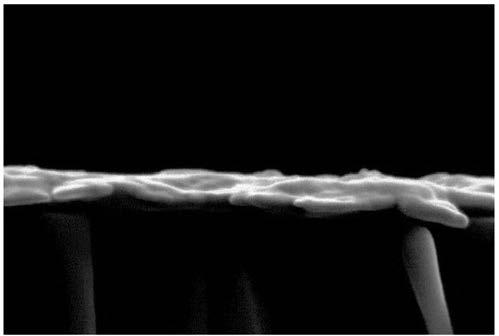
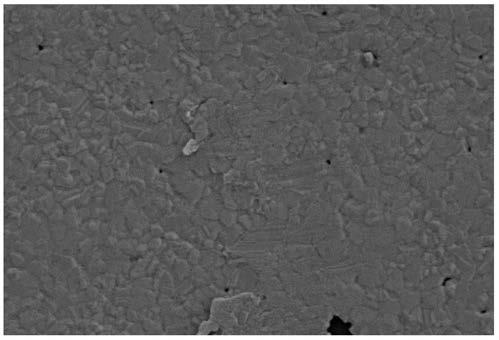
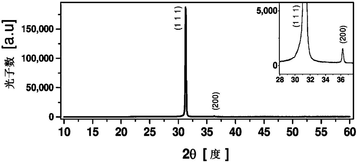
[0222] In all three cases, shiny Pb metal layers with controlled thickness were obtained. Powder X-ray diffraction (XRD) and scanning electron microscope (SEM) images (

[0223] Figures 1A-1D ) and concentration optimization with about 50 or about 120 nm thick evaporated Pb to roughly optimize the morphology.

[0224] The evaporated Pb layer was placed in vials containing 0.05-0.1 M methylammonium iodide (MAI), methylammonium bromide (MABr) and formamidine iodide (FAI) in various alcoholic solutions. The methanol solution of MAI reacts very quickly and essentially etches the layer from the substrate. Ethanol MAI transforms the shiny silver-gray Pb layer into a black coating. ...

Embodiment 2

[0236] Embodiment 2 MAX (X=Br, I) concentration is to MAPbX 3 Effect of film morphology

[0237] The effect of MAX(X=Br,I) concentration on the film morphology is shown below.

[0238] Figures 4A-4E Five different concentrations of MAX are shown: 500 mM, 200 mM, 100 mM, 50 mM and 20 mM. Two effects of increasing the salt concentration are directly seen to be a decrease in crystal size and an increase in the inhomogeneity of the film. Another effect is that cracking of the film occurs at higher concentrations. For solar cell use, the optimum between large crystals and good coverage (smaller crystals) occurs at a concentration of 50-70 mM.

[0239]Membrane morphology is very important in determining membrane properties. The desired morphology depends on the intended use of the film or material.

Embodiment 3

[0240] Embodiment 3 temperature and solvent are to MAPbX 3 Effect of film morphology

[0241] Lower temperature treatments provided better overall coverage ( Figure 7C ), while higher temperatures give on average larger and more anisotropic crystals ( Figure 5 ). Treatment with ethanol instead of IPA resulted in larger crystals but with poorer coverage ( Figure 10A ,10B).


PUM

PropertyMeasurementUnit
thicknessaaaaaaaaaa
thicknessaaaaaaaaaa
thicknessaaaaaaaaaa

Abstract

This invention is related to a method for the preparation of halide perovskite or perovskite-related materials on a substrate and to optoelectronic devices and photovoltaic cells comprising the perovskites prepared by the methods of this invention. The method for the preparation of the perovskite includes a direct conversion of elemental metal or metal alloy to halide perovskite or perovskite-related materials.

Description

technical field [0001] The present invention relates to methods of preparing halide perovskites or perovskite-related materials on substrates, and optoelectronic devices and photovoltaic cells comprising perovskites prepared by the methods of the invention. Methods to prepare perovskites involve the direct conversion of elemental metals or metal alloys into halide perovskites or perovskite-related materials. Background technique [0002] Halide perovskite semiconductors have shown unusually rapid progress in photovoltaic performance, with conversion efficiencies now exceeding 20%. Although these materials have been known for a long time, only in the past 25 years or so have they been seriously considered as electronic materials, especially as light-emitting devices and transistors [1], and their entry into photovoltaic research has only occurred Several years ago (2012) [2-5]. [0003] The most studied material is MAPbI 3 , because the bandgap of this material (approximat...

Claims


Application Information

Patent Timeline
Patent Type & Authority Applications(China)
IPC IPC(8): C23C22/02C23C8/08H01L31/0392H01L31/04C07F7/00C25D3/30C25D3/34C23C14/16C23C14/34C30B25/00C30B29/12C23C18/31
CPCC07F7/2284C07F7/2288C25D3/30C25D3/34C23C8/40C30B7/14C30B25/00C30B29/12C23C18/31Y02E10/549C25D5/48C23C18/1689C07F7/24H10K85/00H10K85/60H10K30/151H10K85/50H10K2102/00C01G21/16C01P2002/34
Inventor D·卡恩G·霍兹Y·拉基塔N·柯德姆
Owner YEDA RES & DEV CO LTD
Why Eureka
Try Eureka