
Direct white LED chip manufacturing method with high thermal stability

A LED chip, high thermal stability technology, applied in the direction of semiconductor devices, electrical components, circuits, etc., can solve the problems of LED light efficiency reduction, reliability reduction, poor thermal stability, etc., to improve the overall color temperature consistency and improve space color Uniformity, the effect of improving process integration

Inactive Publication Date: 2019-03-29
HUAZHONG UNIV OF SCI & TECH
View PDF3 Cites 8 Cited by
  • Summary
  • Abstract
  • Description
  • Claims
  • Application Information

AI Technical Summary

Problems solved by technology

[0004] However, further research shows that: First, because the phosphor powder glue is prone to particle precipitation and local concentration changes during curing, it is difficult to control the uniformity of the phosphor layer during actual processing, and it will affect the repeatability and light color consistency of white LEDs On the other hand, for white LEDs, especially high-power white LED chips, the heat generated by the chip and the secondary heat generated by the phosphor during the light conversion process are both very large, due to the thermal conductivity of the organic phosphor powder Low efficiency and poor thermal stability lead to serious problems such as aging, yellowing and carbonization under long-term thermal radiation and light exposure, and cause LEDs to have reduced luminous efficacy, light color shift and reduced reliability

Method used


Image

  • Direct white LED chip manufacturing method with high thermal stability
  • Direct white LED chip manufacturing method with high thermal stability
  • Direct white LED chip manufacturing method with high thermal stability

Examples


Embodiment 1

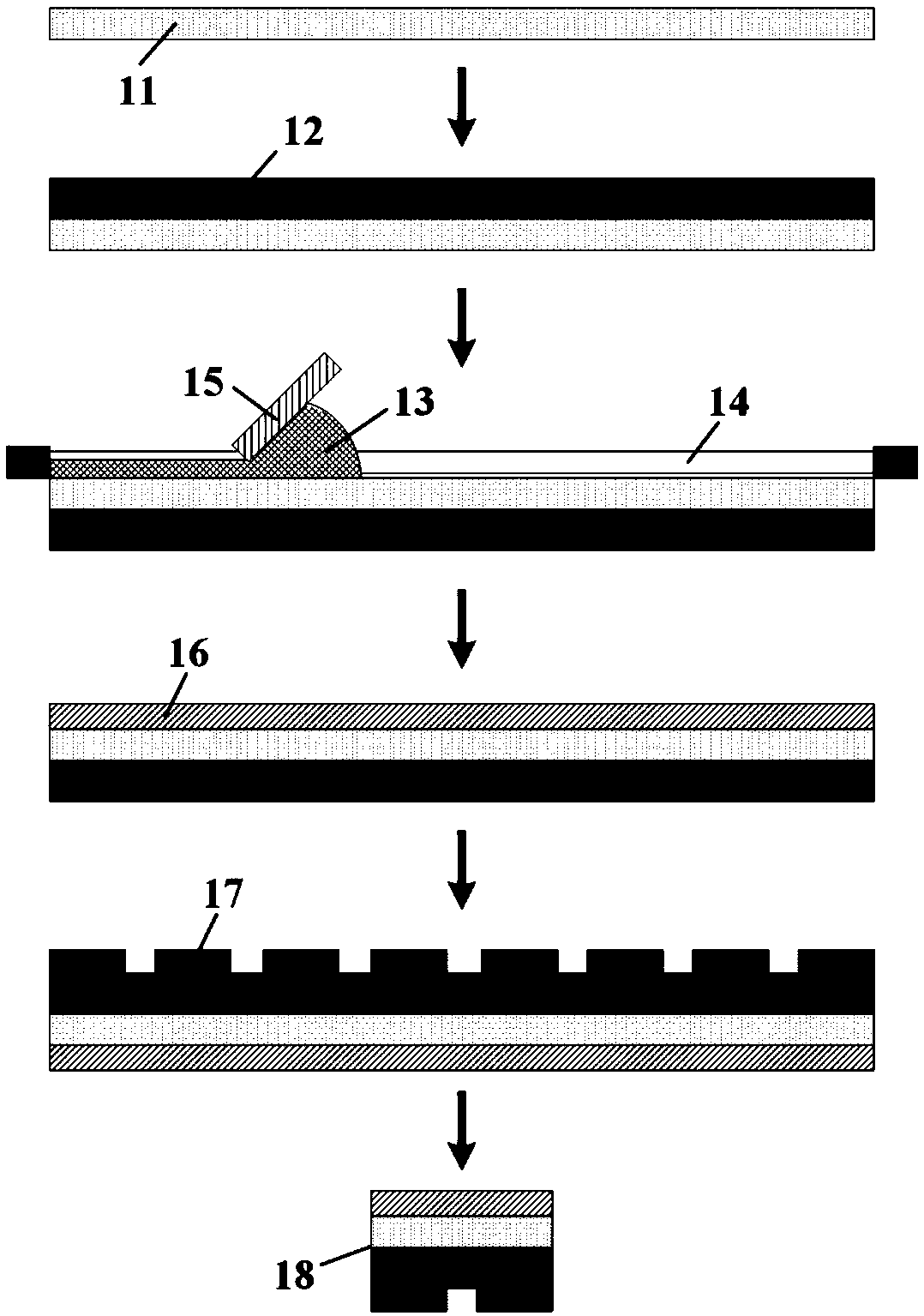
[0055] see figure 1 , this embodiment 1 provides a highly thermally stable direct white light LED chip structure, which includes a sapphire substrate 11 , an epitaxial layer 12 , electrodes and pads 17 , and a fluorescent glass layer 16 . The epitaxial layer 12 is fabricated on the sapphire substrate 11, electrodes and pads 17 are fabricated on the epitaxial layer 12, and the fluorescent glass layer 16 is directly fabricated on the back of the sapphire substrate 11 through coating and low-temperature sintering process.

[0056] The direct white light LED chip manufacturing method of present embodiment 1, it comprises the following steps:

[0057] Step 1, obtaining a blue LED epitaxial layer 12 by epitaxial growth on the sapphire substrate 11;

[0058] Step 2: Coat fluorescent glass paste 13 with a thickness of 100 μm on the back of sapphire substrate 11 by screen printing, and adjust the uniformity of printing thickness by controlling the distance between screen screen plate ...

Embodiment 2

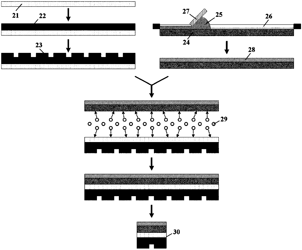
[0064] see figure 2 , this embodiment provides another highly thermally stable direct white LED chip structure, which includes a sapphire substrate 21, an epitaxial layer 22, electrodes and pads 23, and a fluorescent glass layer 28 (including a base 24). The epitaxial layer 22 is made on the sapphire substrate 21, the electrodes and pads 23 are made on the epitaxial layer 22, the fluorescent glass layer 28 is first made on the substrate 24 by coating and low-temperature sintering process, and then activated by surface plasma The bonding process bonds to the back of the sapphire substrate 21 .

[0065] The manufacturing method of the present embodiment comprises the following steps:

[0066] Step 1, on the sapphire substrate 21, obtain the epitaxial layer 22 of the ultraviolet LED by epitaxial growth, and then utilize chip processing technology (photolithography, etching, deposition, etc.) to make electrodes and pads 23 (p, n electrodes and gold-tin pads ), so as to obtain t...

Embodiment 3

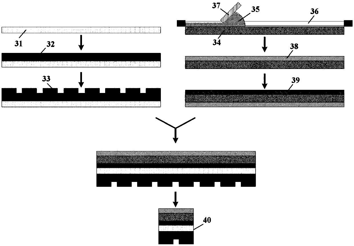
[0079] refer to image 3 , This embodiment provides another highly thermally stable direct white LED chip structure, which includes a sapphire substrate 31, an epitaxial layer 32, electrodes and pads 33, and a fluorescent glass layer 38 (including a substrate 34). The epitaxial layer 32 is made on the sapphire substrate 31, the electrodes and pads 33 are made on the epitaxial layer 32, the fluorescent glass layer 38 is first made on the substrate 34 by coating and low-temperature sintering process, and then bonded by adhesive The process is bonded to the back of the sapphire substrate 31 .

[0080] The manufacturing method corresponding to this embodiment includes the following steps:

[0081] Step 1, on the sapphire substrate 31, obtain the epitaxial layer 32 of the blue LED by epitaxial growth, and then utilize chip processing technology (photolithography, etching, deposition, etc.) to make electrodes and pads 33 (p, n electrodes and gold-tin soldering Disk), so as to obta...


PUM

PropertyMeasurementUnit
Glass transition temperatureaaaaaaaaaa
Surface roughnessaaaaaaaaaa
Glass transition temperatureaaaaaaaaaa

Abstract

The invention belongs to the technical field of semiconductor manufacturing and discloses a direct white LED chip manufacturing method with high thermal stability. The method comprises steps that firstly, an LED epitaxial layer is prepared on a sapphire substrate through epitaxial growth, secondly, fluorescent glass paste is coated on a back side of the sapphire substrate, a fluorescent glass layer is obtained through low-temperature sintering, thirdly, electrodes and pads are made on the epitaxial layer, and lastly, through thinning and polishing the fluorescent glass layer and shredding, thedirect white LED chip is obtained; or firstly, the LED wafer and the fluorescent glass piece are prepared, secondly, the fluorescent glass piece is bonded to the sapphire substrate through the bonding process, and lastly, the wafer is cut to obtain the direct white LED chip. The method is advantaged in that the phosphor coating process in the process of white LED manufacturing is avoided, the thickness of the phosphor layer is uniform, production efficiency and color consistency of the white LED are improved, a problem of poor thermal reliability of the phosphor is solved, and the thermal stability of the white LED is improved.

Description

technical field [0001] The invention belongs to the related field of semiconductor manufacturing technology, and more specifically relates to a method for manufacturing a direct white LED chip with high thermal stability. Background technique [0002] A light emitting diode (Light Emitting Diode, LED) is an electroluminescent semiconductor device that utilizes the interband transition radiation recombination of electrons and holes to emit light. Compared with traditional lighting sources such as incandescent lamps and fluorescent lamps, LEDs have the advantages of high luminous efficiency, long life, environmental protection and energy saving, and compact structure. They are considered to be a new generation of green lighting sources. Among them, white LED has been widely used in lighting and backlight display and other fields, such as road lighting, indoor lighting, car headlights, TV backlights, mobile phone flashlights, etc. [0003] For the manufacturing process of whit...

Claims


Application Information

Patent Timeline
IPC IPC(8): H01L33/00H01L33/50
CPCH01L33/005H01L33/502H01L33/505H01L2933/0041
Inventor 陈明祥彭洋牟运罗小兵刘胜
Owner HUAZHONG UNIV OF SCI & TECH
Learn More