Full titanium nitride current collector/electrode supercapacitor and preparation method thereof
A technology of supercapacitors and current collectors, applied in the manufacture of hybrid/electric double layer capacitors, hybrid capacitor electrodes, hybrid capacitor current collectors, etc., can solve the problems of frequency response (poor rate characteristics, etc., and achieve strong process applicability and simple process. Ease of use and a wide variety of effects to choose from
- Summary
- Abstract
- Description
- Claims
- Application Information
AI Technical Summary
Problems solved by technology
Method used
Image
Examples
Embodiment example 1
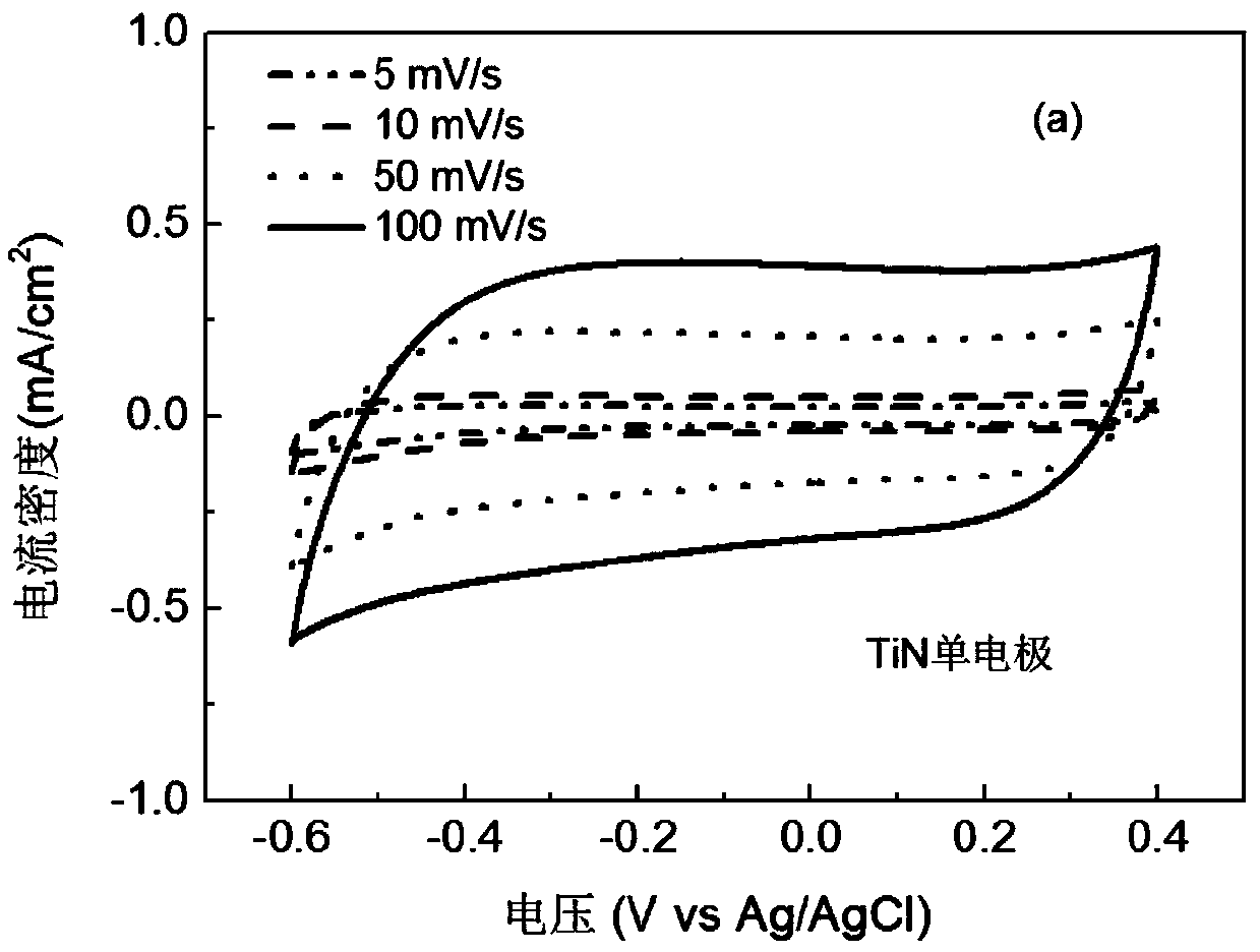
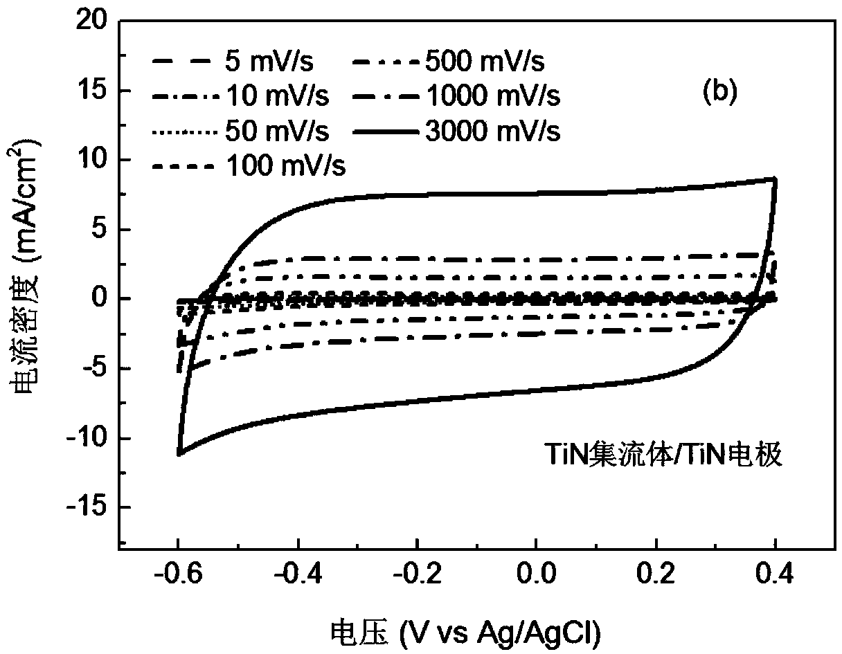
[0031] In this embodiment, a single crystal silicon substrate is selected as the substrate, and the semiconductor industry standard RCA cleaning process is used for cleaning. DC reactive magnetron sputtering is adopted, the target material is titanium metal, the base distance of the target is 20cm, Ar:N 2=10:1sccm, sputtering power: 100W, substrate temperature: 400°C, working pressure: 0.2Pa, substrate bias: -50V, sputtering time: 15min, first deposit a layer with a thickness of 85nm, and a resistivity of 110μΩ·cm , the surface is smooth and dense TiN thin film is used as the current collector material, and then the distance between the target and the base is 20cm, Ar:N 2 =10:1sccm, sputtering power: 100W, substrate temperature: 400°C, working pressure: 0.4Pa, sputtering time: grow a layer of thickness 240nm under the conditions of 30min, resistivity 2500μΩ·cm, loose and porous TiN film as electrode material. Using a three-electrode test system, the working electrode is TiN,...
Embodiment example 2
[0033] In this embodiment, a single crystal silicon substrate is selected as the substrate, and the semiconductor industry standard RCA cleaning process is used for cleaning. Using DC reactive magnetron sputtering, the target material is titanium metal, the base distance of the target is 50cm, Ar:N 2 =20:1sccm, sputtering power: 200W, substrate temperature: 200°C, working pressure: 0.2Pa, substrate bias: -50V, sputtering time: 15min, deposit a layer with a thickness of 55nm first, and a resistivity of 120μΩ·cm , a smooth and dense TiN thin film is used as the current collector material. Then at a base distance of 20cm, Ar:N 2 =10:1sccm, sputtering power: 100W, substrate temperature: 400°C, working pressure: 0.4Pa, sputtering time: grow a layer of thickness of 280nm under the conditions of 30min, resistivity of 2500μΩ·cm, loose and porous TiN film as electrode material. Using a three-electrode test system, the working electrode is TiN, the counter electrode is platinum elect...
Embodiment example 3
[0035] In this embodiment, a single crystal silicon substrate is selected as the substrate, and the semiconductor industry standard RCA cleaning process is used for cleaning. Using radio frequency reactive magnetron sputtering, the target material is titanium metal, the target base distance is 60cm, Ar:N 2 =20:1sccm, sputtering power: 150W, substrate temperature: 150℃, working pressure: 0.8Pa, substrate bias voltage: -200V, sputtering time: 10min, first deposit a layer with a thickness of 25nm, and a resistivity of 100μΩ·cm , the surface is smooth and dense TiN thin film is used as the current collector material, and then the distance between the target and the base is 60cm, Ar:N 2 =20:1sccm, sputtering power: 200W, substrate temperature: 200°C, working pressure: 0.8Pa, sputtering time: grow a layer with a thickness of 330nm and resistivity of 4100μΩ·cm under the conditions of 30min, loose and porous TiN film as electrode material. Using a three-electrode test system, the wo...
PUM
| Property | Measurement | Unit |
|---|---|---|
| Thickness | aaaaa | aaaaa |
| Resistivity | aaaaa | aaaaa |
| Resistivity | aaaaa | aaaaa |
Abstract
Description
Claims
Application Information


