
Method for preparing nanometer silicon carbide at low temperature

A nano-silicon carbide, low-temperature technology, applied in the fields of silicon carbide, chemical instruments and methods, carbides, etc., can solve the problems of easy agglomeration and low yield, and achieve the effect of simple process and convenient large-scale production.

Active Publication Date: 2019-05-14
NORTHEASTERN UNIV
View PDF4 Cites 5 Cited by
  • Summary
  • Abstract
  • Description
  • Claims
  • Application Information

AI Technical Summary

Problems solved by technology

However, this method has extremely high requirements on the purity of raw materials, and the obtained product has a wide range of particle size distribution, is easy to agglomerate, and has a low yield.
Therefore, how to find a method for preparing nano-SiC with simple process, high yield, high purity, and controllable particle size and structure is still a big challenge.

Method used


Image

  • Method for preparing nanometer silicon carbide at low temperature
  • Method for preparing nanometer silicon carbide at low temperature
  • Method for preparing nanometer silicon carbide at low temperature

Examples


Embodiment 1

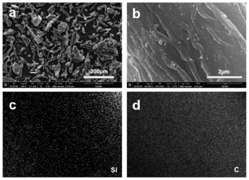
[0027] The first confinement effect: Weigh a certain amount of cellulose and nano-silica (mass ratio is 3:1), put it in a 100ml ball mill jar, mill it at 450rpm for 2h, and then put the mixture in a tube furnace for pyrolysis treatment . The treatment temperature is 600°C, the time is 4h, and the heating rate is 5°C min -1 . The obtained sample was naturally cooled to room temperature to obtain a silica / carbon composite. figure 1 (a) and (b) are scanning electron microscope pictures of the silicon dioxide / carbon composite prepared in this embodiment, from figure 1 In the energy spectrum scanning images of (c) and (d), it can be seen that silicon is evenly distributed on the carbon skeleton, forming a good composite structure with the carbon skeleton.

[0028] The second confinement effect: mechanically mix the silica / carbon composite obtained above with metal magnesium according to a certain mass ratio (1:1), then transfer the mixture to a stainless steel reactor, and final...

Embodiment 2

[0030] The first confinement effect: the same as in Embodiment 1.

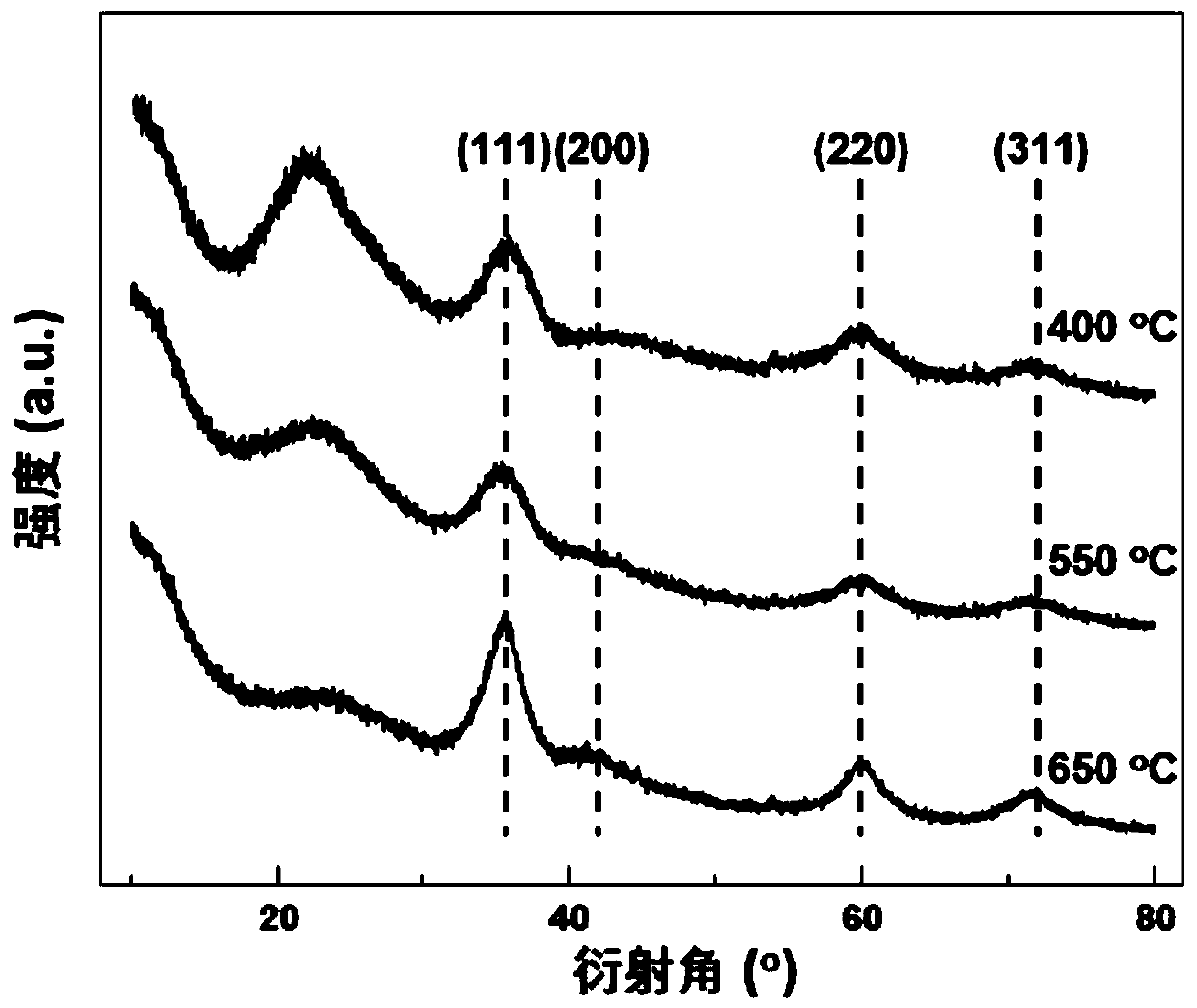
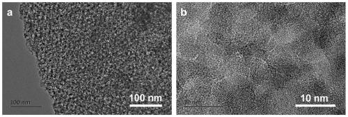
[0031] The second confinement effect: the reduction temperature is 650°C, other conditions are the same as in Example 1, and the XRD diffraction pattern of the obtained nano-SiC is as follows figure 2 As shown, compared with the standard card JCPDS29-1129, its 2θ=35.6°, 60° and 71.7° correspond to the (111), (220) and (311) crystal planes of SiC, respectively. image 3 (a) and (b) are the TEM images of the sample, respectively. It can be seen that the sample has a certain pore structure at low resolution, which is mainly due to the SiO 2 Pores left after deoxygenation reacts with the carbon skeleton. The (111) interplanar spacing of SiC can be measured as 0.252nm in the high-resolution transmission electron microscope pictures. Figure 4 It is a scanning electron microscope picture of the sample, and it can be seen that it has an obvious mesoporous structure. Figure 5 (a) is the nitrogen adsorption-desorp...

Embodiment 3

[0033] The first confinement effect: the same as in Example 1.

[0034] The second confinement effect: the reduction temperature is 400°C, other conditions are the same as in Example 1, and the XRD diffraction pattern of the obtained nano-SiC is as follows figure 2 As shown, compared with the standard card JCPDS29-1129, its 2θ=35.6°, 60° and 71.7° correspond to the (111), (220) and (311) crystal planes of SiC, respectively.


PUM

PropertyMeasurementUnit
particle diameteraaaaaaaaaa
lattice spacingaaaaaaaaaa

Abstract

The invention provides a method for preparing nanometer silicon carbide at a low temperature. The method adopts the 'double confinements' process and comprises the following steps: firstly preparing asilicon dioxide / carbon compound through the pyrolysis of a silicon dioxide / polymer compound; then mechanically mixing the obtained compound with magnesium metal / calcium and performing thermal treatment in a closed reactor; finally sequentially cleaning with hydrochloric acids and hydrofluoric acids to obtain the nano-structured SiC. In a synthetic route, a carbon skeleton in the silicon dioxide / carbon compound provides a first confinement effect to confine the growth of the nanometer silicon carbide, and the closed reactor provides a second confinement effect to reduce the carbothermal reduction temperature. The nanometer silicon carbide prepared by the method has large specific surface area and abundant porosity, can load a metallic silver catalyst as a carrier and is used for a lithiumion battery anode material. The method for preparing the nanometer silicon carbide, provided by the invention, is simple in process and convenient for realization of large-scale production.

Description

technical field [0001] The invention belongs to the field of material preparation and relates to a method for preparing nano silicon carbide at low temperature. Background technique [0002] Silicon carbide (SiC), commonly known as corundum, is a new type of semiconductor material developed following the first-generation semiconductor materials and second-generation compound semiconductor materials. It has a wide band gap (2.3eV-3.3eV), high thermal conductivity, and fast electron mobility. And other advantages, so it is very suitable for making electronic devices with high temperature, high power and high density integration. In addition, SiC also has excellent chemical stability, good mechanical properties, and thermal shock resistance, making it an ideal candidate for filter materials and catalyst supports under harsh conditions. Nanostructured SiC has better performance than traditional SiC powder, can meet the strict requirements of higher technical fields, and has wid...

Claims


Application Information

Patent Timeline
Patent Type & Authority Applications(China)
IPC IPC(8): C01B32/97B82Y40/00H01M4/58H01M10/0525B01J32/00
CPCY02E60/10
Inventor 孙蔷王增榕
Owner NORTHEASTERN UNIV
Learn More