Metal micro/nano wire array and preparation method thereof

A nanowire array, metal technology, applied in metal material coating process, microstructure technology, microstructure device and other directions, can solve the problem of unable to obtain high aspect ratio micro/nanowires, etc., achieve high recycling rate, improve The effect of specific surface area

Inactive Publication Date: 2019-05-24
NANJING UNIV
View PDF9 Cites 4 Cited by
  • Summary
  • Abstract
  • Description
  • Claims
  • Application Information

AI Technical Summary

Problems solved by technology

[0005] Therefore, the technical problem to be solved by the present invention is to overcome the defects in the prior art that micro / nano wires with high aspect ratio cannot be obtained, thereby providing a metal micro / nano wire array and its preparation method

Method used


Image

  • Metal micro/nano wire array and preparation method thereof
  • Metal micro/nano wire array and preparation method thereof
  • Metal micro/nano wire array and preparation method thereof

Examples


Embodiment 1

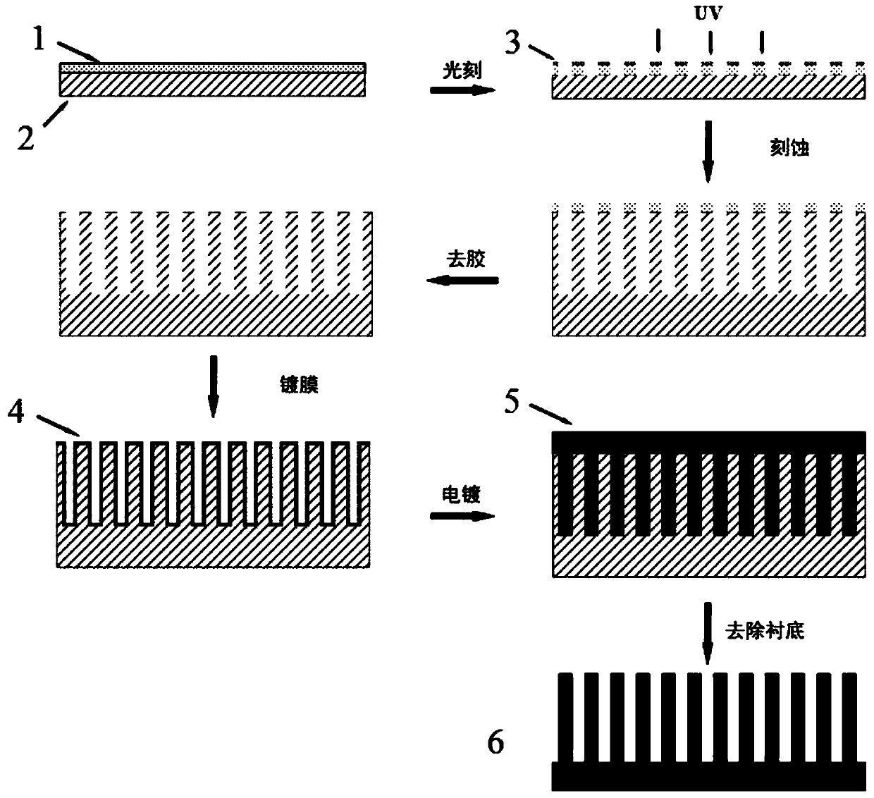
[0042] This embodiment provides a method for preparing nickel micron line arrays by photolithography micro-nano processing technology, such as figure 1 Shown is the flow chart of the present embodiment method, and concrete steps are as follows:

[0043] Preparation of silicon micron deep holes: ordinary silicon wafers are spin-coated with photoresist at a rate of 4000r / min for 40s and a film thickness of 1.5μm. A photolithographic template with a diameter of 2 μm and a period of 6 μm was used for photolithography to obtain photoresist holes with a diameter of 2 μm and a period of 6 μm. Use photoresist as a mask to perform deep silicon etching (Northern Huachuang HSE200 deep silicon etching machine), and the etching gas is SF 6 , the shielding gas is C 4 f 8 , the etching rate is 0.2μm / s, the etching time is 120s, and the etching depth is 20μm. Use acetone to ultrasonically remove the photoresist on the surface of the structure for 5 minutes to obtain silicon micron deep hol...

Embodiment 2

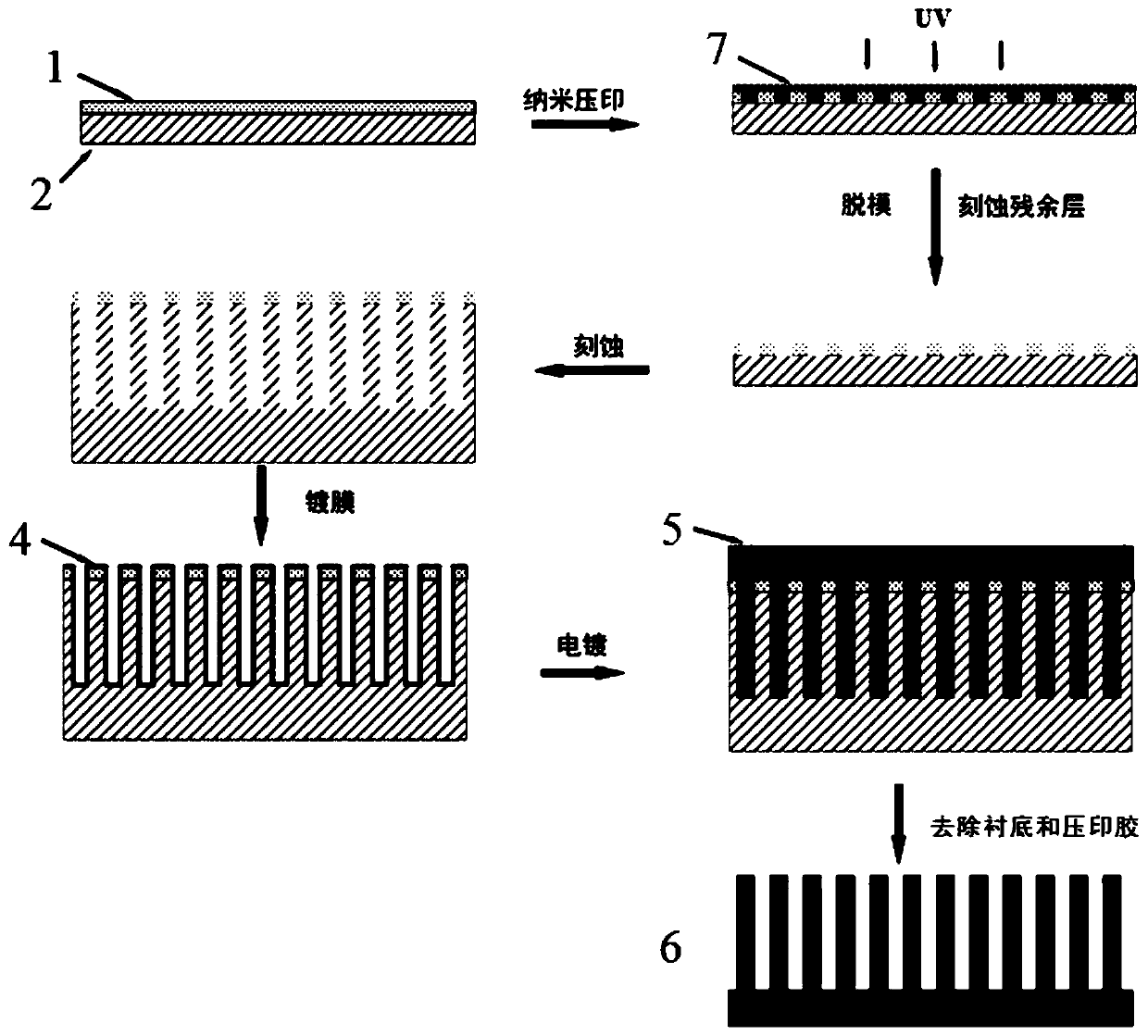
[0048] This embodiment provides a method for preparing nickel nanowire arrays by nanoimprinting technology, such as figure 2 Shown is the flow chart of the present embodiment method, and concrete steps are as follows:

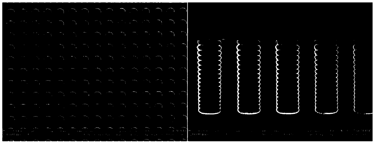
[0049] Preparation of silicon nano-deep holes: Ordinary silicon wafers are spin-coated with UV-curable imprinting glue, the speed is 2000r / min, the time is 40s, the film thickness is 150nm, and the PDMS soft template with a diameter of 500nm and a period of 1000nm is used for imprinting. After UV-curing , forming embossed glue holes with a diameter of 500nm and a period of 1000nm, and using an inductively coupled plasma etching machine (ULVAC CE300I) to etch and remove the residual layer. Use imprinting glue as a mask to perform deep silicon etching, and the etching gas is SF 6 , the shielding gas is C 4 f 8 , the etching rate is 0.2 μm / s, the etching time is 60 s, and the etching depth is 10 μm. Obtain silicon nano-deep pores, such as Figure 5 shown.

...

Embodiment 3

[0054] This embodiment provides a method for preparing a copper micron line array by photolithography micro-nano processing technology, and the specific steps are as follows:

[0055] Preparation of silicon micron deep holes: ordinary silicon wafers are spin-coated with photoresist at a rate of 3000r / min for 40s and a film thickness of 1.8μm. A photolithographic template with a diameter of 5 μm and a period of 10 μm was taken for photolithography to obtain photoresist holes with a diameter of 5 μm and a period of 10 μm. Use photoresist as a mask for deep silicon etching, and the etching gas is SF 6 , the shielding gas is C 4 f 8 , the etching rate was 0.15 μm / s, the etching time was 400 s, and the etching depth was 40 μm. The photoresist on the surface of the structure was removed by ultrasonication of acetone for 5 minutes, and silicon micron deep holes were obtained.

[0056] Preparation of metallic copper micron wires: Evaporate a layer of metallic copper on the surface ...


PUM

PropertyMeasurementUnit
diameteraaaaaaaaaa
thicknessaaaaaaaaaa
diameteraaaaaaaaaa

Abstract

The invention belongs to the technical field of micro-nano machining, and particularly relates to a metal micro / nano wire array and a preparation method thereof. The metal micro / nano wire array comprises a supporting layer metal sheet and metal micro / nano wires erected on the metal sheet. The metal micro / nano wire array has a large depth-to-width ratio, and the diameter and height of the metal micro / nano wire and the thickness of the metal sheet can be accurately controlled; The metal micro / nano wires are directly erected on the metal sheets and are not crossed and overlapped with one another,so that the specific surface area and the repeated utilization rate are increased; The metal micro / nano-wire array can be applied to preparation of a flexible nano device with a large depth-to-widthratio. According to the preparation method, a material with relatively good rigidity and etching stability is used as a substrate, so that the problems of collapse and the like in an etching process can be avoided, and a micro / nano wire array with a high depth-to-width ratio is obtained; In addition, according to the method, the height of the micro / nano wire can be accurately controlled by controlling the etching time.

Description

technical field [0001] The invention belongs to the technical field of micro-nano processing, and in particular relates to a metal micro / nano wire array and a preparation method thereof. Background technique [0002] Metal micro / nanowires with large specific surface area have excellent physical and chemical properties, especially the large surface area, which can greatly improve the catalytic efficiency when the metal is used as the catalyst; in addition, when the surface of the metal micro / nanowire is loaded with active substances, it shows excellent performance. The performance of the pseudocapacitive electrode has a very good development prospect in the supercapacitor current collector device. [0003] At present, the preparation of metal micro / nanowires is usually synthesized and grown by chemical methods, and the obtained metal micro / nanowires have disadvantages such as uncontrollable morphology and poor reusability, while the micro / nanowires prepared by micro-nano proc...

Claims


Application Information

Patent Timeline
Patent Type & Authority Applications(China)
IPC IPC(8): B81B3/00B81C1/00
Inventor 郝宗斌傅欣欣张良葛海雄袁长胜崔玉双
Owner NANJING UNIV
Why Eureka
Try Eureka