Preparation method of MoSe2 in-plane homogeneous p-n junction

An n-type, field-effect transistor technology, applied in semiconductor/solid-state device manufacturing, electrical components, circuits, etc., can solve problems such as long time consumption, weak interaction force, and hindering TMDCs doping

Inactive Publication Date: 2019-07-26
CENT SOUTH UNIV
View PDF7 Cites 3 Cited by
  • Summary
  • Abstract
  • Description
  • Claims
  • Application Information

AI Technical Summary

Problems solved by technology

However, in MoSe 2 In p-type doping, the way of direct exposure to air or pure oxygen takes a long time, and because the interaction force between the adsorbed gas and TMDCs is weak, the doping effect will gra

Method used


Image

  • Preparation method of MoSe2 in-plane homogeneous p-n junction
  • Preparation method of MoSe2 in-plane homogeneous p-n junction
  • Preparation method of MoSe2 in-plane homogeneous p-n junction

Examples


preparation example Construction

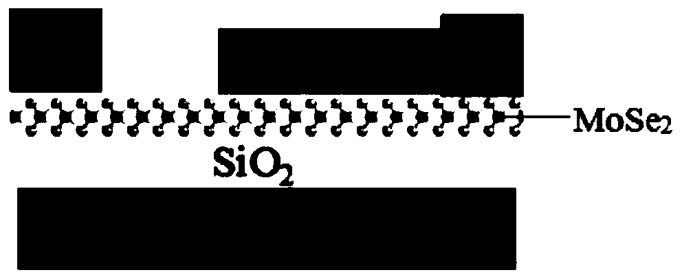
[0033] The present invention provides a MoSe 2 A method for preparing an in-plane homogeneous p-n junction, comprising the steps of:

[0034] (1) Provide MoSe 2 Field Effect Transistor;

[0035] (2) along the perpendicular to the MoSe 2 The direction of the field effect transistor electrode protects part of the channel close to the source or drain, and the partially protected MoSe 2 Field Effect Transistor;

[0036] (3) The partially protected MoSe 2 Field-effect transistors undergo UV-ozone treatment to obtain MoSe 2 In-plane homogeneous p-n junction.

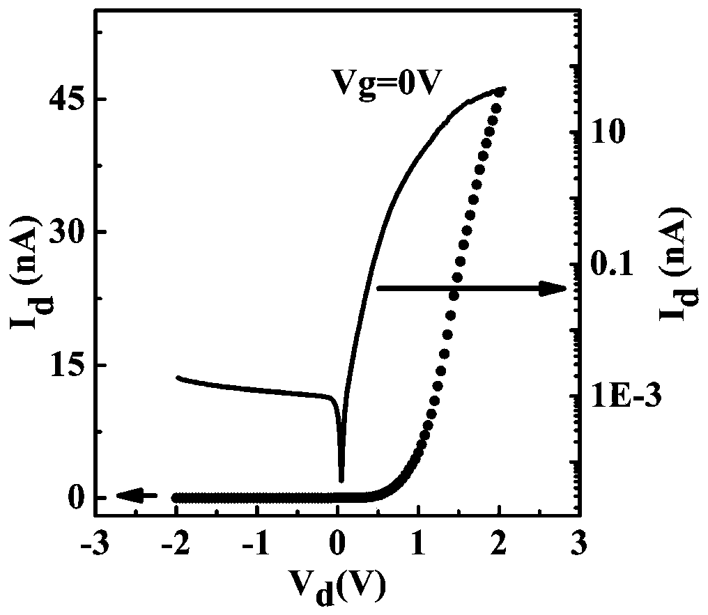
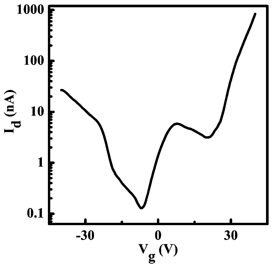
[0037] The present invention uses MoSe 2 A part of the field effect transistor channel is protected, and then treated with ultraviolet ozone, and the exposed channel is under the strong oxidation of ultraviolet ozone, MoSe 2 MoO with high work function will be formed on the surface x , resulting in electrons from MoSe with lower work function 2 Transfer to MoO x , so the exposed MoSe 2 It shows hole conduction, whi...

Embodiment 1

[0073] Select n-type SiO with 300nm thick oxide layer 2 / Si as the substrate, wash the substrate in an ultrasonic oscillator with deionized water, acetone, and isopropanol in sequence, then dry the substrate with a nitrogen gun, and place it on a hot plate at 90 °C for later use;

[0074] A little bulk MoSe 2 Placed on the blue film tape, folded in half repeatedly 6 times until the MoSe 2 Uniformly distributed on the tape, MoSe will stick 2 The tape aligns the SiO 2 / Si substrate is pasted on, after repeated extrusion with a beaker, the tape is peeled off, MoSe with different layers 2 Randomly distributed on SiO 2 / Si, in n-type SiO 2 / Si substrate to get MoSe 2 layers; few-layer MoSe can be discerned using an optical microscope that can coordinate 2, and then further determine the number of layers by Raman spectroscopy, which is 5 to 6 layers;

[0075] In the MoSe 2 Spin-coat PMMA glue (molecular weight: 950K) on the layer at a speed of 4000r / min. After spin-coating ...


PUM

PropertyMeasurementUnit
Thicknessaaaaaaaaaa
Thicknessaaaaaaaaaa
Thicknessaaaaaaaaaa

Abstract

The invention provides a preparation method of a MoSe2 in-plane homogeneous p-n junction, and belongs to the technical field of semiconductor materials. According to the method, partial channels of aMoSe2 field-effect transistor are protected, then ultraviolet ozone treatment is carried out, and the exposed channel is under the strong oxidation effect of ultraviolet ozone, and the surface layer of MoSe2 forms MoOx with a high-work function, so that electrons are transferred from the MoSe2 with relatively low work function to MoOx, the exposed MoSe2 shows hole conduction, and the protected region is still electrically conductive, and therefore electrons and holes in the same channel are electrically conductive simultaneously, and the MoSe2 in-plane homogeneous p-n junction is obtained. Experimental results show that, the rectification characteristic and the double Dirac point of the product prepared by the method disclosed by the invention are typical characteristic of the p-n junction, so that it shows that a p-n junction is successfully prepared; and the MoSe2 in-plane homogeneous p-n junction obtained by the method has obvious response to illumination.

Description

technical field [0001] The invention relates to the technical field of semiconductor materials, in particular to a MoSe 2 Fabrication method of in-plane homogeneous p-n junction. Background technique [0002] In recent years, two-dimensional (2D) transition metal chalcogenides (TMDCs) have shown great application prospects in many fields such as optoelectronic devices, energy, and catalysis due to their unique electrical, optical, and other physical properties. However, monolayer / few-layer (FL) TMDCs grown by mechanical exfoliation and chemical vapor deposition (CVD) exhibit a single n-type or p-type, which is due to the MoSe 2 A lot of defects are generated, and the defects can cause the Fermi surface to be pinned near the conduction band or the valence band. Logic devices are complementary devices, which need to contain both n-type and p-type, so it is very challenging to realize the application of 2DTMDCs. The p-n junction is widely used in photodetection and light-emi...

Claims


Application Information

Patent Timeline
IPC IPC(8): H01L21/322H01L29/06H01L29/24H01L29/78
CPCH01L21/322H01L29/0684H01L29/24H01L29/78
Inventor 黄寒郑晓明刘金鑫施姣肖君婷陈凤鸣
Owner CENT SOUTH UNIV
Why Eureka
Try Eureka