

Junction barrier Schottky diode with a floating field ring terminal structure and a preparation method thereof
A junction barrier Schottky and terminal structure technology, applied in the direction of diodes, semiconductor/solid-state device manufacturing, electrical components, etc., can solve the problems of low device breakdown voltage, large reverse leakage current, temperature sensitivity, etc. Reduce the effect, avoid electric field concentration, and improve the effect of reverse breakdown characteristics
- Summary
- Abstract
- Description
- Claims
- Application Information
AI Technical Summary
Problems solved by technology
Method used
Image

Examples
preparation example Construction
[0042] The present invention also provides a method for preparing a junction barrier Schottky diode with a floating field ring termination structure, which specifically includes:
[0043] Step 1: Deposit the first epitaxial layer on the substrate, and deposit the second epitaxial layer on the first epitaxial layer; the deposition method is not particularly limited, and the organic chemical vapor deposition method well known in the art can be used. Before the substrate is used, it is preferable to clean it with acetone methanol and deionized water to remove organic contamination on the substrate;
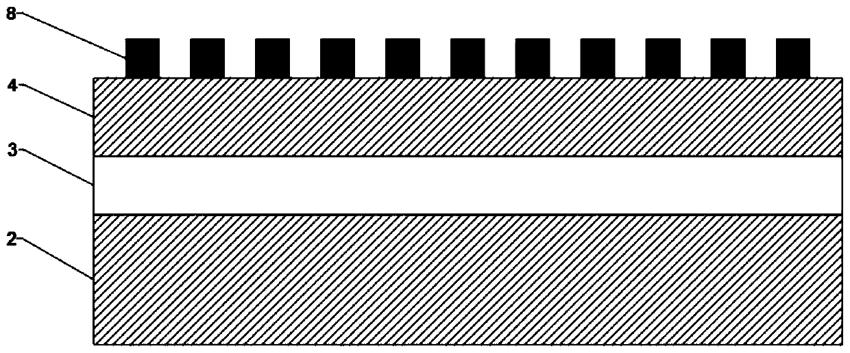
[0044] Step 2: Perform a photolithography process on the second epitaxial layer to form an ion implantation region, and then prepare a P-type region barrier layer. The thickness of the P-type region barrier layer is preferably 2-4 μm, and then ion implant Mg + , in a high-pressure nitrogen atmosphere, magnesium ions are activated through repeated annealing, and the barrier layer is r...
Embodiment 1
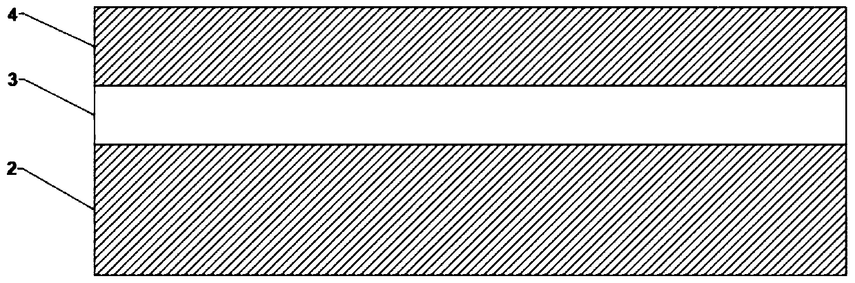
[0050] Step 1: If figure 1 , a schematic diagram of the growth of GaN-based JBS materials, the preparation process includes: prepare a double-sided polished n-type highly doped self-supporting GaN substrate 2, and use acetone, methanol and deionized water to ultrasonically clean for 10 minutes to remove organic contamination on GaN ; On the n-type highly doped free-standing GaN substrate 2, the n of the first epitaxial layer 2 μm is deposited + type GaN3, the carrier concentration is about 1.5x10 18 cm -3 , the second epitaxial layer is 23μm n-type GaN4, the carrier concentration is about 8x10 15 cm -3 ;Such as figure 1 As shown, specifically:
[0051] 1) Use HCl:H 2 Soak in O (1:5 volume ratio) dilute hydrochloric acid for 2 minutes to remove the surface oxide layer on the GaN surface due to long-term placement in the air, use deionized water to remove the residual acid on the surface, and use N 2 Blow dry and quickly put into the cavity of MOCVD;
[0052] 2) Vacuumiz...
PUM
| Property | Measurement | Unit |
|---|---|---|
| Thickness | aaaaa | aaaaa |
| Thickness | aaaaa | aaaaa |
| Width | aaaaa | aaaaa |
Abstract
Description
Claims
Application Information