Solar cell with composite dielectric passivation layer structure and preparation process thereof

A technology of solar cells and preparation process, which is applied in the field of PERC solar cells, can solve the problems of easily damaged passivation film layer, increased manufacturing cost, and decreased electrical performance, so as to improve the stability and reliability of anti-light decay and anti-PID performance, increase short-circuit current and open-circuit voltage, and enhance the effect of comprehensive utilization

Pending Publication Date: 2019-11-15
TONGWEI SOLAR ENERGY CHENGDU CO LID +2
View PDF0 Cites 36 Cited by
  • Summary
  • Abstract
  • Description
  • Claims
  • Application Information

AI Technical Summary

Problems solved by technology

However, due to the -OH and -CH3 groups that may exist in the alumina dielectric film layer, if the annealing process is not strictly matched, it may react with the H in the SixNy:H stack from the capping stack during sintering , so that the passivation effect of the laminated passivation film will be destroyed under the high temperature condition of the back-end sintering (>860°C), resulting in a decrease in electrical performance and the generation of defective EL detection films; at the same time, after a period of time, certain light and temperature conditions Combination accumulation may leave secondary reactants to gather and escape, resulting in LID / LeTID phenomenon in PERC batteries
The cause of the LeTID phenomenon is complex, and many research institutions such as SCHOTT, UNSW, Konstan University, ISFH, and Aalto University are in the process of further research. The current mainstream view is that hydrogen is the main factor, and metal ions such as B-O / FeB and Cu in raw materials are The resulting attenuation is also more serious
[0006] Therefore, the current industrialized PERC solar cells generally have problems such as easy damage to the passivation film layer, serious back-end attenuation, and abnormal EL; The matching of chemical film structure design and module packaging materials such as POE can reduce the PID attenuation of EVA-packaged double-sided PERC modules to a certain extent. Anti-PID performance, improving the above stability and reliability of PERC batteries is becoming more and more important
[0007] However, since the double-sided battery combined with PID is a new product failure phenomenon that has appeared in recent years, and there are ambiguities and multi-factor constraints in the mechanism, inducing conditions, and influencing factors of the original PID phenomenon, the matching of component packaging materials will definitely To a certain extent, the back-end manufacturing cost is increased, so solar cell manufacturers are more inclined to reduce the PID failure phenomenon of industrialized PERC series solar cells through the design of the front-end dielectric film structure of the battery and the optimized combination of the process formula

Method used


Image

  • Solar cell with composite dielectric passivation layer structure and preparation process thereof
  • Solar cell with composite dielectric passivation layer structure and preparation process thereof
  • Solar cell with composite dielectric passivation layer structure and preparation process thereof

Examples


preparation example Construction

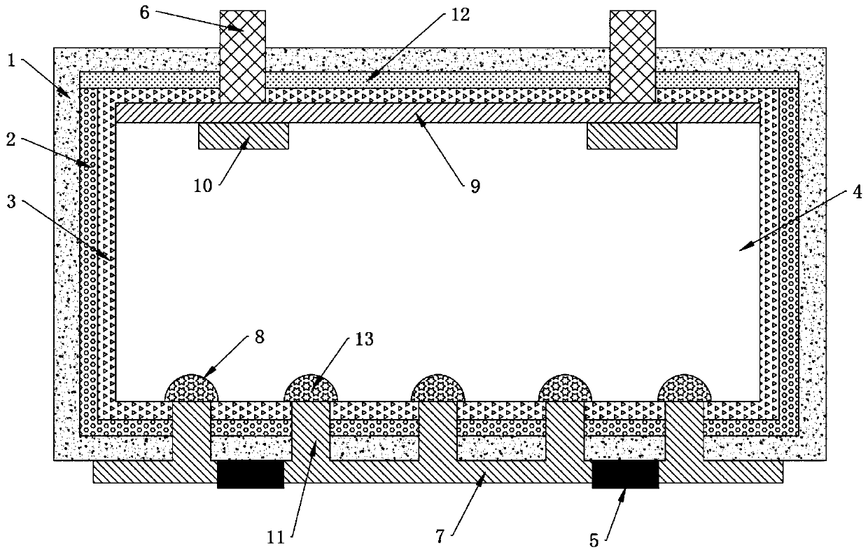
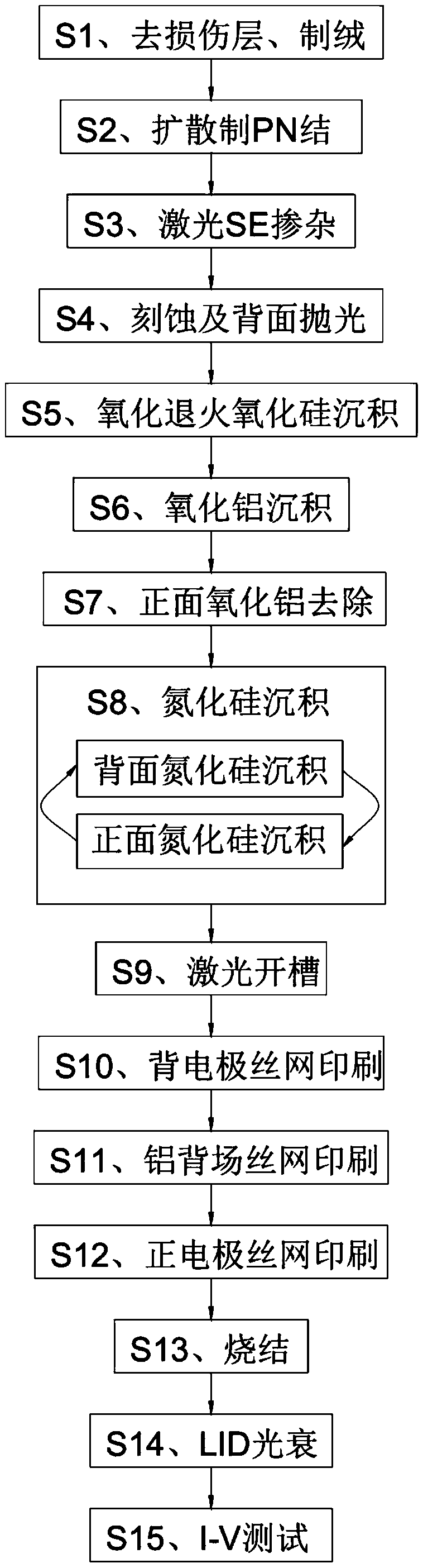
[0072] A preparation process for a solar cell with a composite dielectric passivation layer structure, in which a silicon oxide film 3 and an aluminum oxide film 2 are sequentially deposited on the front, back and peripheral surfaces of a P-type silicon substrate, and the front aluminum oxide film 2 is washed away and deposited Higher n-value silicon nitride or silicon oxynitride film 12, and then deposit low n-value silicon nitride film 1 on both sides and the periphery to form a laminated composite dielectric passivation layer, and laser doping on the front side to form N++SE The heavily doped area 10 is matched with the Ag positive electrode 6 printed and penetrated through the passivation film layer, and a window is partially opened on the back side for electrode derivation. The specific steps are as follows:

[0073] S1. Removing the damaged layer and making texture: pre-clean and texture the P-type silicon substrate 4, remove the damaged layer 3-5um on the surface of the ...

Embodiment 1

[0091] The present invention comprises the following specific steps:

[0092] (1) Remove the mechanical damage layer 4um on the surface of the single crystal P-type silicon substrate 4 with a NaOH solution with a concentration of 40g / L, clean the silicon chip surface, and simultaneously anisotropize the silicon chip surface with 18g / L NaOH liquid Corrosion, forming 2-3um inverted pyramid suede texture;

[0093] (2) In the diffusion furnace tube, POCl is used 3 Negative pressure diffusion of liquid source forms P-N junction, diffusion temperature is 830°C, process time is 55min, diffusion sheet resistance is controlled at 130-150ohm / port;

[0094] (3) Laser SE doping: On the diffused silicon wafer, the phosphorous atoms on the diffused surface phosphosilicate glass are laser doped by 5.6% in the subsequent screen-printed main grid and fine grid electrode areas, Form a local heavily doped region, the dense diffusion region sheet resistance 70-80ohm / ㎡;

[0095] (4) Using HF: H...

Embodiment 2

[0108] The present invention comprises the following specific steps:

[0109] (1) remove the mechanical damage layer 3.5um on the surface of the single crystal P-type silicon substrate 4 with a concentration of 30g / L NaOH solution, clean the silicon chip surface, and simultaneously use 20g / L of NaOH liquid to this silicon chip surface Anisotropic corrosion, forming 3-4um inverted pyramid suede texture;

[0110] (2) In the diffusion furnace tube, POCl is used 3 The liquid source is diffused under negative pressure to form a P-N junction, the diffusion temperature is 850°C, the process time is 45 minutes, and the diffusion sheet resistance is controlled at 140-170ohm / port;

[0111] (3) Laser SE doping: On the diffused P-type silicon substrate 4, the phosphorus atoms on the diffused surface phosphosilicate glass are laser doped in the subsequent screen-printed main grid and fine grid electrode regions by laser. Doping 5.2%, forming a local heavily doped region, the sheet resist...


PUM

PropertyMeasurementUnit
thicknessaaaaaaaaaa
thicknessaaaaaaaaaa
thicknessaaaaaaaaaa

Abstract

The invention discloses a solar cell with a composite dielectric passivation layer structure and a preparation process thereof. A silicon oxide film, an alumina film and a silicon nitride or silicon oxynitride film are deposited in turn on the front, back and sides of a p-type silicon substrate to form a composite dielectric film on the whole surface, and windows are opened locally to lead electrodes out. Through aluminum oxide, silicon dioxide, silicon oxynitride, silicon nitride with different refractive indexes and a back surface passivation layer with a laminated structure of the materials, the back surface recombination rate is greatly reduced, the back reflectivity is improved, the CTM of a module is reduced, and the light attenuation and heat-assisted light attenuation and the anti-PID performance of the cell are improved. The structure can be made on a boron/gallium-doped p-type monocrystalline silicon, p-type polycrystalline silicon or p-type monocrystalline-silicon-like substrate, and a passivation method based on the composite dielectric film passivation structure can be used to manufacture PERC cells, double-sided PERC+ cells and imbricate PERC cells. Based on the preparation process steps and sequence, the corresponding preparation mode and the process parameter range of the laminated structure, the making of the cell can be well completed.

Description

technical field [0001] The invention relates to the technical field of PERC solar cells, in particular to a solar cell with a composite dielectric passivation film layer structure and a preparation process thereof. Background technique [0002] Photovoltaic power generation is a way to effectively utilize solar energy by directly converting sunlight energy into electrical energy through the photovoltaic effect of semiconductors, reducing the consumption loss between energy conversions, and then supplying the generated electricity to users. Photovoltaic power generation can reduce the proportion of petrochemical energy use, thereby reducing carbon emissions and improving the environment. After more than ten years of technical catching up, it has gradually become an emerging strategic manufacturing industry that can rival developed countries such as Europe, America, and Japan; at the same time, photovoltaic power generation is also the country's targeted poverty alleviation. O...

Claims


Application Information

Patent Timeline
Patent Type & Authority Applications(China)
IPC IPC(8): H01L31/0216H01L31/04H01L31/18
CPCH01L31/02168H01L31/04H01L31/184Y02E10/544Y02P70/50
Inventor 王岚张忠文杨蕾谢毅苏荣
Owner TONGWEI SOLAR ENERGY CHENGDU CO LID
Why Eureka
Try Eureka