

Terahertz wave radiation source based on graphene material
A technology of graphene and hertzian waves, applied in the field of terahertz waves, can solve the problems of complex components of terahertz waves, low conversion efficiency, and high preparation precision, and achieve the effects of simple composition, improved conversion efficiency, and high conversion efficiency
- Summary
- Abstract
- Description
- Claims
- Application Information
AI Technical Summary
Problems solved by technology
Method used
Image

Examples
Embodiment 1
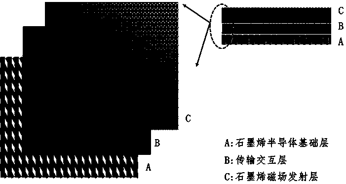
[0024] First, chemical vapor deposition is used to construct the graphene semiconductor base layer, and then the Fermi energy level of graphene is adjusted by chemical nitrogen doping to realize the graphene semiconductor characteristics, and then transferred to polyester PET film to form a conductive network layer with a certain structure. Its graphene is mainly composed of single-layer graphene and a small amount of multi-layer graphene, forming the semiconductor base layer A.
[0025] The preferred metal compound for the transmission and interaction layer is TiO 2 Nano oxide layer, bonding resin is high density polyethylene material. The material ratio and basic parameters of the transmission interactive layer are as follows: transition metal compound powder 15 wt%, binder resin 45 wt%, dispersed coupling agent 2 wt%, conductive agent 38 wt%, the thickness of the transmission layer is 0.4 mm, marked as Layer B.
[0026] The graphene magnetic field emission layer in the te...
Embodiment 2
[0029] Electrodeposition is used to structure the graphene semiconductor base layer, and nitrogen doping is added by adding melamine during the electrodeposition process, which is directly transferred to the epoxy resin sheet and processed to form a conductive network layer of the structure. The active graphene monolayer rate in the electrodeposition solution reaches 90%, and the others are multi-layer graphene, forming the semiconductor base layer A.
[0030] The preferred metal compound for the transmission and interaction layer is TiO 2 Nano oxide layer, bonding resin is high density polyethylene material. The material ratio and basic parameters of the transmission interactive layer are as follows: 20 wt% transition metal compound powder, 40 wt% binder resin, 2 wt% dispersed coupling agent, 0.5 wt% conductive agent, the thickness of the transmission layer is 0.4 mm, marked as Layer B.
[0031] The graphene magnetic field emission layer in the terahertz wave source has a m...
Embodiment 3
[0034] The graphene slurry is printed into the ceramic substrate by screen printing, and the graphene is modified by introducing metal nano-elements by electroplating, and then processed to form a conductive network layer of the structure. The single-layer ratio in the graphene slurry reaches 99%, and the others are multi-layer graphene, which constitutes the semiconductor base layer A.
[0035] The preferred metal compound for the transmission and interaction layer is CaCO 3 The nano oxide layer and the bonding resin are low temperature resistant materials. The material ratio and basic parameters of the transmission interactive layer are as follows: 20 wt% transition metal compound powder, 40 wt% binder resin, 2 wt% dispersed coupling agent, 0.5 wt% conductive agent, the thickness of the transmission layer is 0.4 mm, marked For the B layer.
[0036] The graphene magnetic field emission layer in the terahertz wave source has a monolayer ratio of 80% of the material. Graphene...
PUM
| Property | Measurement | Unit |
|---|---|---|
| Thickness | aaaaa | aaaaa |
| Power | aaaaa | aaaaa |
Abstract
Description
Claims
Application Information