

LCP high-frequency substrate having high-Dk and low-Df characteristic and fabrication method thereof
A substrate and high-frequency technology, which is applied in the field of high-frequency and high-transmission substrates and preparation, can solve the problems that cannot really meet high-frequency and high-speed, cannot meet high Dk requirements, and is prone to high leakage current, etc., to achieve good UV laser drilling capabilities , good mechanical properties, low rebound effect
- Summary
- Abstract
- Description
- Claims
- Application Information
AI Technical Summary
Problems solved by technology
Method used
Image


Examples
Embodiment approach
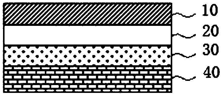
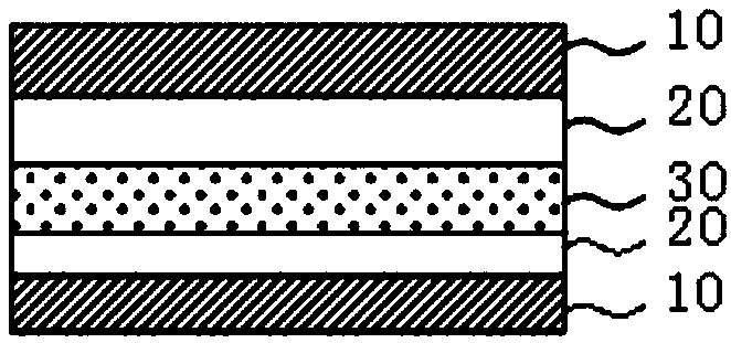
[0051] Embodiment: A LCP high-frequency substrate with high Dk and low Df characteristics, such as Figure 1 to Figure 3 As shown, including at least one copper foil layer, at least one high dielectric LCP (liquid crystal polymer) core layer and at least one high dielectric adhesive layer, the high dielectric LCP core layer is located between the copper foil layer and the high dielectric adhesive layer Among them, the high dielectric LCP core layer refers to a core layer with a Dk (dielectric constant) value of 6-100 (10GHz), and a Df (dielectric loss factor) value of 0.002-0.010 (10GHz), the A high dielectric adhesive layer refers to an adhesive layer with a Dk value of 6-100 (10GHz) and a Df value of 0.002-0.010 (10GHz);
[0052] The thickness of the copper foil layer is 1-35 μm; the thickness of the high dielectric LCP core layer is 12-100 μm, and the thickness of the high dielectric glue layer is 12-100 μm.
[0053] The high dielectric adhesive layer has a bonding strengt...
Embodiment approach 1
[0070] Embodiment 1: An LCP high-frequency substrate with high Dk and low Df characteristics, such as figure 1As shown, the LCP high-frequency substrate is a single-sided copper-clad substrate, and the single-sided copper-clad substrate includes a copper foil layer, a high dielectric LCP core layer and a high dielectric adhesive layer, and the high dielectric LCP The core layer is located between the copper foil layer and the high dielectric adhesive layer, and the thickness of the single-sided copper-clad substrate is 25-235 μm.
[0071] In this embodiment, the single-sided copper-clad substrate further includes a release layer, and the release layer is located on the surface of the high-dielectric adhesive layer.
[0072] The release layer can be a release film whose material is at least one of polypropylene, biaxially oriented polypropylene and polyethylene terephthalate, and can be a release film with double-sided release capability. film, or use release paper.
[0073] ...
Embodiment approach 2
[0077] Embodiment 2: An LCP high-frequency substrate with high Dk and low Df characteristics, such as figure 2 As shown, the LCP high-frequency substrate is a double-sided copper-clad substrate, and the double-sided copper-clad substrate includes two copper foil layers, two high-dielectric LCP core layers and a high-dielectric adhesive layer, and the double-sided clad The copper substrate consists of copper foil layer, high dielectric LCP core layer, high dielectric glue layer, high dielectric LCP core layer and copper foil layer from top to bottom, and the thickness of the double-sided copper clad substrate is 38-370 μm.
[0078] The preparation method of embodiment 2 comprises the following steps:
[0079] Step 1. Coating the precursor of the high-dielectric LCP core layer on one side of the copper foil layer, removing the solvent at 60-180°C, and annealing at 250°C for 10 hours to obtain two semi-finished products A;
[0080] Step 2, coating the precursor of the high diel...
PUM
| Property | Measurement | Unit |
|---|---|---|
| Thickness | aaaaa | aaaaa |
| Thickness | aaaaa | aaaaa |
| Thickness | aaaaa | aaaaa |
Abstract
Description
Claims
Application Information