Distributed feedback laser of monolithic integrated silicon optical chip and preparation method thereof

A distributed feedback and silicon photonics chip technology, applied in the direction of lasers, laser components, semiconductor lasers, etc., can solve the problems of CMOS process incompatibility, low optical coupling efficiency, complex preparation process, etc., to achieve complete CMOS process compatibility, The effect of compact device structure and mature manufacturing process

Active Publication Date: 2020-04-10
FUDAN UNIV
View PDF5 Cites 7 Cited by
  • Summary
  • Abstract
  • Description
  • Claims
  • Application Information

AI Technical Summary

Problems solved by technology

Although the hybrid integration of external light sources has high luminous efficiency and good laser properties, the integration level is low, the preparation process is complicated, it is not compatible with CMOS technology, and the coupling and alignment of beams is difficult, resulting in high cost of the final system; The biggest difficulty is the low gain coefficient problem caused by free carrier absorption and increased optical loss. It is difficult to achieve short-range optical amplification in the case of free carrier injection; silicon germanium lasers use heavy doping and material strain to modulate germanium However, the team at the Massachusetts Institute of Technology found that further research is still needed in terms of integration process and low light outcoupling efficiency due to the high refractive index of germanium; III-V lasers Bonding integration and direct silicon-based growth need to grow a buffer material layer or bonding layer of several microns or even tens of microns on the silicon substrate, which will adversely affect the planarization of the chip, and the heating effect will seriously reduce the performance of the integrated device

Method used


Image

  • Distributed feedback laser of monolithic integrated silicon optical chip and preparation method thereof
  • Distributed feedback laser of monolithic integrated silicon optical chip and preparation method thereof
  • Distributed feedback laser of monolithic integrated silicon optical chip and preparation method thereof

Examples


Embodiment Construction

[0043] The following examples are used to illustrate the present invention, but not to limit the present invention.

[0044] 1. Raw material and formula

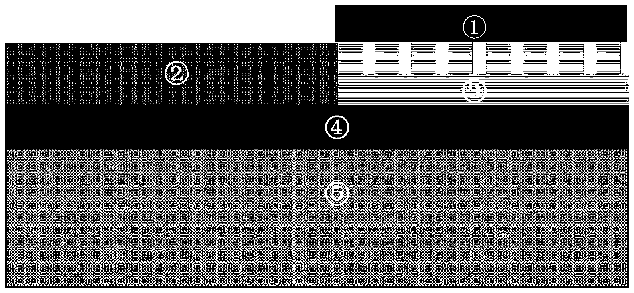
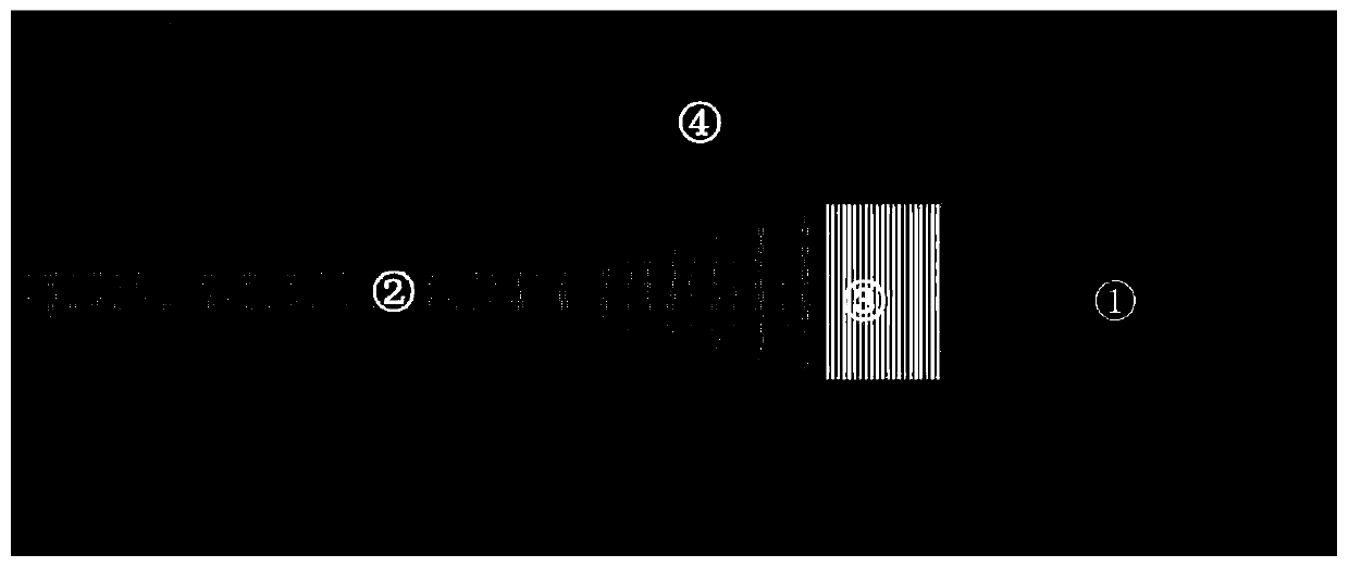
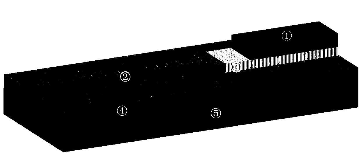
[0045] Substrate: polished on both sides, volume is 20×20×0.2mm 3 SOI substrate;

[0046] Doping solvent: MIBK, Shanghai Aladdin Biochemical Technology Co., Ltd.;

[0047] Doping solute: ErI 3 , Shanghai Aladdin Biochemical Technology Co., Ltd.;

[0048] Gain Materials: Dow Corning FOx-1x and FOx-2x Flowable Oxides, Dow Corning Corporation;

[0049] Substrate cleaning solution: alcohol (analytical grade), acetone (analytical grade), Sinopharm Chemical Reagent Co., Ltd.;

[0050] Photoresist cleaning agent: phosphoric acid (analytical grade), hydrogen peroxide (analytical grade), concentrated sulfuric acid, Sinopharm Chemical Reagent Co., Ltd.

[0051] 2. Production device

[0052] Plasmalab System 120 Inductively Coupled Plasma Etcher, Oxford Instruments Ltd;

[0053] SK2-4-12 program-controlled tubular resistance fu...


PUM

PropertyMeasurementUnit
thicknessaaaaaaaaaa
thicknessaaaaaaaaaa
lengthaaaaaaaaaa

Abstract

The invention belongs to the technical field of silicon light, and particularly relates to a distributed feedback laser of a monolithic integrated silicon light chip and a preparation method thereof.The laser structure comprises a silicon substrate of an SOI substrate, a silica insulating layer, a doped silicon nanocrystalline thin film layer with high laser gain, and a silicon waveguide etched by a top intrinsic silicon substrate, wherein the doped silicon nanocrystalline thin film layer comprises a one-dimensional distribution feedback structure, and a Bragg grating is formed through adoption of a photoetching technology to form the resonant cavity of the laser; a light source serving as an optical pump is an electrically excited LED or laser diode, is directly attached to the upper portion of the laser area of the optical pump, and generates laser output in an optical pumping mode; and an emergent laser is directly aligned with the silicon waveguide on the SOI, so that the very high coupling efficiency is obtained. The device is compact in structure, mature in manufacturing process and low in signal laser and waveguide coupling loss, and the defects that a silicon-based laser integrated structure based on a semiconductor gain material is complex, and waveguide and laser coupling is difficult are overcome.

Description

technical field [0001] The invention belongs to the technical field of silicon photonics, and in particular relates to a laser device with a single-chip integrated silicon photonics chip and a preparation method thereof. Background technique [0002] The invention of the transistor is an epoch-making event in the 20th century, which pushed the development speed of human civilization to an unprecedented height. Silicon-based microelectronic devices have gradually realized the advantages of low power consumption, low cost, and easy integration during the past few decades of development, quickly occupying most of the electronic market and becoming the cornerstone of the information revolution era. However, further reductions in the size of microelectronic devices have brought to the fore problems with silicon materials such as channeling. At the same time, the increase of metal interconnection delay and energy consumption is also the main reason hindering the rapid development...

Claims


Application Information

Patent Timeline
Patent Type & Authority Applications(China)
IPC IPC(8): H01S5/04H01S5/12H01S5/30H01S5/026
CPCH01S5/026H01S5/041H01S5/12H01S5/3031
Inventor 张驰张树宇陆明吴翔
Owner FUDAN UNIV
Why Eureka
Try Eureka