
Treatment method for improving surface pollution of LED chip

A technology for LED chips and surface pollution, which is applied in semiconductor devices, electrical components, circuits, etc., can solve the problems of abnormal surface of aluminum electrodes, susceptibility to acid and alkali corrosion, and difficult welding wires, etc., so as to improve product yield and avoid surface abnormalities , The effect of less raw material consumption

Active Publication Date: 2020-05-01
SHANDONG INSPUR HUAGUANG OPTOELECTRONICS
View PDF12 Cites 4 Cited by
  • Summary
  • Abstract
  • Description
  • Claims
  • Application Information

AI Technical Summary

Problems solved by technology

At present, the metal electrode material on the surface of the LED chip electrode in the industry is mainly gold or aluminum. Compared with the aluminum electrode, the gold electrode is better in terms of stability and quality, but the cost is high. Therefore, most LED manufacturers still choose aluminum electrodes as the electrode material. Aluminum is lively. , is susceptible to acid and alkali corrosion, and is more sensitive to the acid-base reaction of the solution and the environment. This is the main reason why aluminum electrodes are prone to surface abnormalities. Of course, it is also related to the surface roughness of electrode evaporation.
In addition, during the normal chip production process, due to the multi-step organic and inorganic reagents and hot nitrogen drying operations, the chip surface is also prone to contamination such as reagent residues, which cannot be effectively removed by ordinary secondary cleaning.
Conventional methods to deal with surface pollution of LED chips are mainly to remove surface pollutants by using organic solvents to clean or physically bombard the chip surface with a glue machine, etching machine, etc., but the effect is limited and often brings new quality problems. In the end, most chips cannot escape the result of quality degradation, and the cost and efficiency affected by the processing method are also a loss
[0005] So far, no reports have been found on the improvement methods for surface abnormalities such as LED chip contamination, roughness, and difficult soldering.

Method used


Image

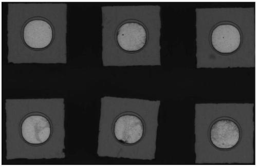
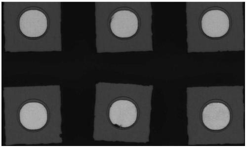
  • Treatment method for improving surface pollution of LED chip
  • Treatment method for improving surface pollution of LED chip

Examples


Embodiment 1

[0031] A treatment method for improving surface pollution of LED chips, comprising the steps of:

[0032] (1) Clean the chip in an absolute ethanol solution with a purity of 99.7% for 15 seconds, then take it out and use a wool brush dipped in absolute ethanol to gently scrub the surface of the chip, scrub the entire chip surface 3 times, and then place the chip on Rinse under deionized water for 10s with a conductivity of 0.2μs / cm;

[0033] (2) Place the chip in an aqueous solution of 5% acetic acid (purity 99.6%) by volume and clean it for 3 minutes, then take it out and use a wool brush to dip the acetic acid aqueous solution to gently scrub the surface of the chip, scrub the entire chip surface 3 times, and then Rinse the chip under deionized water for 12s;

[0034] (3) Place the chip in a mixed solution composed of acetic acid (purity 96%), hypochlorous acid (purity 97%), ammonium fluoride (purity 97%), and deionized water (the weight ratio is 2% acetic acid, hypochlorou...

Embodiment 2

[0039] A treatment method for improving surface pollution of LED chips, comprising the steps of:

[0040] (1) Clean the chip in an absolute ethanol solution with a purity of 99.8% for 12 seconds, then take it out and use a wool brush dipped in absolute ethanol to gently scrub the surface of the chip, scrub the entire chip surface twice, and then place the chip on The conductivity is 0.18μs / cm and rinsed in deionized water for 14s;

[0041] (2) Place the chip in an aqueous solution of 3% acetic acid (99.7% purity) by volume and clean it for 4 minutes, then take it out and use a wool brush to dip in the acetic acid aqueous solution to gently scrub the surface of the chip, scrub the entire chip surface 4 times, and then Rinse the chip under deionized water for 20s;

[0042] (3) Place the chip in a mixed solution composed of oxalic acid (purity 99%), hydrogen sulfuric acid (purity 96%), sodium fluoride (purity 98%), and deionized water (the weight ratio is oxalic acid 6%, hydroge...

Embodiment 3

[0047] A treatment method for improving surface pollution of LED chips, comprising the steps of:

[0048] (1) Clean the chip in an absolute ethanol solution with a purity of 99.7% for 26 seconds, then take it out and use a wool brush dipped in absolute ethanol to gently scrub the surface of the chip, brush the entire chip surface 6 times, and then place the chip on The conductivity is 0.17μs / cm and rinsed under deionized water for 20s;

[0049] (2) Clean the chip in an aqueous solution of 8% acetic acid (99.8% purity) by volume for 2 minutes, then take it out and use a wool brush to dip in the aqueous solution of acetic acid to gently scrub the surface of the chip. The entire chip surface is scrubbed twice, and then Rinse the chip under deionized water for 21s;

[0050] (3) Place the chip in a mixed solution consisting of hypochlorous acid (purity 96%), hydrofluoric acid (purity 97%), ammonium fluoride (purity 95%), sodium bifluoride (purity 98%), and deionized water (The weig...


PUM


Abstract

The invention relates to a treatment method for improving surface pollution of an LED chip and belongs to the technical field of the LED chip. The method comprises steps of (1) sequentially placing achip in absolute ethyl alcohol solution and the deionized water for cleaning and scrubbing; (2) sequentially placing the chip in acetic acid aqueous solution and the deionized water for cleaning and scrubbing; (3) cleaning the chip in mixed solution consisting of acid, the deionized water and fluoride, taking out the chip, and washing the chip in the deionized water; (4) placing the chip in a cleaning machine for high-pressure deionized water cleaning, and utilizing nitrogen for blow-drying; and (5) taking out the chip and placing the chip on a heating table for baking, and thoroughly removingthe water vapor. The method is advantaged in that the method is less in raw material consumption, simple in steps, simple and convenient to operate, low in processing cost, and capable of effectivelyremoving surface anomalies such as chip surface pollution, residual reagents, roughness and the like, and improves the chip quality and yield.

Description

technical field [0001] The invention relates to a treatment method for improving surface pollution of LED chips, belonging to the technical field of LED chips. Background technique [0002] LED lighting technology has developed very rapidly. Since the 1960s, relevant statistics have shown that the cost of LEDs has dropped tenfold every ten years, while the luminous efficiency has increased tenfold every ten years. At present, it has been used in living lighting, traffic signals, Architectural decoration, landscape, outdoor display, backlight, toys, clothing and other aspects are accepted by people. At the same time, LED technology is constantly upgrading and innovating to meet the different needs of human production and life. [0003] In the production process of LED, the production of LED chips is an important factor affecting product cost, index and sales. As we all know, the production of LED chips needs to go through multiple steps such as metal coating, graphics produc...

Claims


Application Information

Patent Timeline
Patent Type & Authority Applications(China)
IPC IPC(8): H01L21/02H01L33/00
CPCH01L33/005H01L21/02068
Inventor 胡夕伦闫宝华肖成峰
Owner SHANDONG INSPUR HUAGUANG OPTOELECTRONICS
Learn More