

Preparation method of silicon wafer micro-nano turbid transparent composite suede and application thereof
A technology for crystalline silicon wafers and silicon wafer surfaces, which is applied in the field of preparation of micro-nano-turbid composite textured surfaces of crystalline silicon wafers, and can solve the problems of increased cleaning workload, low photoelectric conversion efficiency, and difficulty in processing silicon wafers.
- Summary
- Abstract
- Description
- Claims
- Application Information
AI Technical Summary
Problems solved by technology
Method used
Image

Examples
Embodiment 1
[0040] A method for preparing a micro-nano turbid composite textured surface of a crystalline silicon chip, comprising the following steps:
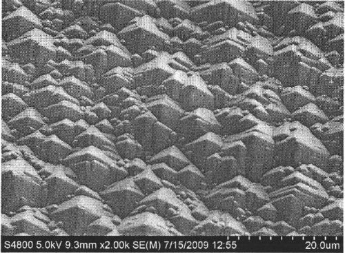
[0041] S1: Fully mix the sand with an average particle size of 10 microns and water to form a micron-sized water-sand mixture, and then use a high-pressure water-sand spray gun to spray the micron-sized water-sand mixture evenly onto the surface of the silicon wafer to form micron-sized grains on the surface of the polycrystalline silicon wafer. surface (such as figure 2 shown);
[0042] S2: Fully stir and mix sand particles with an average particle size of 2 microns and water to form a nano-scale water-sand mixture, and then use a high-pressure water-sand spray gun to uniformly spray the water-sand mixture onto the surface of the polycrystalline silicon wafer obtained in step S1. A nanoscale pockmark layer is formed on the surface of the pockmark layer;
[0043] S3: put the sandblasted polysilicon wafer into the etching solution to e...
Embodiment 20
[0056] A preparation process for solar cells, comprising the following steps:
[0057] S1: Fully mix the sand with an average particle size of 10 microns and water to form a micron-sized water-sand mixture, and then use a high-pressure water-sand spray gun to evenly spray the micron-sized water-sand mixture to the front of the silicon wafer to form a micron-sized hemp surface layer;
[0058] S2: Fully stir and mix the sand particles with an average particle size of 2 microns and water to form a nano-scale water-sand mixture, and then use a high-pressure water-sand spray gun to evenly spray the water-sand mixture to the front of the crystalline silicon wafer formed in step S1, Form nano-scale grained surface layer on the surface of micron grained surface layer;
[0059] S3: sending the crystalline silicon wafer obtained in step 2 into a diffusion furnace for diffusion and junction formation;
[0060] S4: cleaning the crystalline silicon wafer obtained in step S3 to remove imp...
Embodiment 21
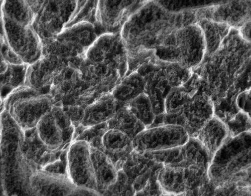
[0066] Such as Figure 8 with Figure 9 Shown, a kind of solar cell sheet, it comprises crystalline silicon sheet 10, the front side 101 of described crystalline silicon sheet has the micro-nano turbid composite suede layer described in embodiment 2, the back side 102 of crystalline silicon sheet has sandblasting process The prepared nano-scale light-trapping fleece layer.
[0067] Such as Figure 9 As shown, when sunlight irradiates the micro-nano composite turbid suede on the surface of the silicon wafer, it produces a very good diffuse reflection effect, so that the sunlight reflects in different angles in all directions in the micro- and nano-concave-convex pits, and refracts into the silicon wafer. The smooth and transparent nano-scale concave-convex surface can not only effectively refract and absorb short-wave light, but also has a strong absorption of red-orange long-wave visible light. The smooth and bright concave mirror effect reduces stray light, and the light re...
PUM
 Abstract
Description
Claims
Application Information