Passivation contact solar cell with selective emitter structure and preparation method of passivation contact solar cell

A solar cell and emitter technology, applied in the field of solar cells, can solve the problems of high activation difficulty, immature boron doping, etc., and achieve the effects of simple and effective preparation method, simple preparation method and improved efficiency

Inactive Publication Date: 2020-05-15
TAIZHOU ZHONGLAI PHOTOELECTRIC TECH CO LTD
View PDF9 Cites 13 Cited by
  • Summary
  • Abstract
  • Description
  • Claims
  • Application Information

AI Technical Summary

Problems solved by technology

[0003] The existing N-type passivated contact cell structure solves the passivation of the n surface, but the recombination of the emitter surface is still relatively high, which has become a bottleneck for efficiency improvement. To reduce the recombination of the emitter surface, it is necessary to take into account the passivation and contact resistance
[0004] Compared with phosphorus-doped emitters, since boron is much more difficult to activate than phosphorus, the selective doping of boron is still a difficult problem in the world, and there is no mass-producible selective emitter preparation method with both efficiency and yield. , such as laser doping, which is very mature in phosphorus selective doping, is still immature in boron doping

Method used


Image

  • Passivation contact solar cell with selective emitter structure and preparation method of passivation contact solar cell
  • Passivation contact solar cell with selective emitter structure and preparation method of passivation contact solar cell
  • Passivation contact solar cell with selective emitter structure and preparation method of passivation contact solar cell

Examples


preparation example Construction

[0045] A kind of passivation contact solar cell preparation method of the present invention, its technical scheme is: comprise the following steps:

[0046] (1), prepare the suede surface on the back surface and the front surface of the N-type crystalline silicon substrate;

[0047] (2) Carry out boron diffusion treatment on the textured surface of the front surface of the N-type crystalline silicon substrate to form a lightly doped region layer;

[0048] (3) Using a mask to perform local boron ion implantation in the lightly doped region layer of the N-type crystalline silicon substrate, and annealing to form a locally heavily doped region;

[0049] (4), preparing a tunneling oxide layer on the textured surface of the back surface of the N-type crystalline silicon substrate treated in step (3), and preparing a phosphorus-doped polysilicon layer on the tunneling oxide layer;

[0050] (5), preparing a silicon nitride anti-reflection layer on the phosphorus-doped polysilicon la...

Embodiment 1

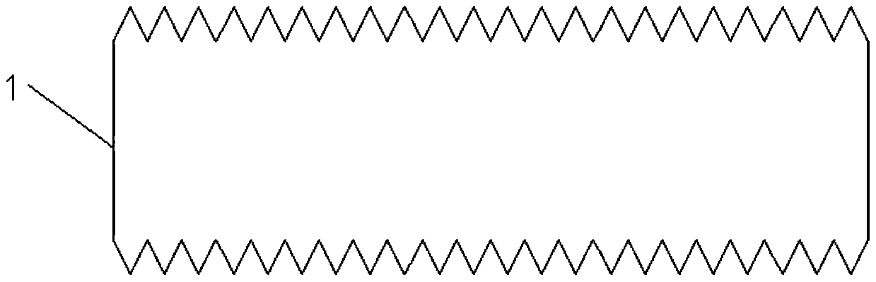
[0072] (1) Take an N-type crystalline silicon substrate 1 with a resistivity of 1Ω·cm and a thickness of 160 μm, and place the N-type crystalline silicon substrate 1 with a resistivity of 1Ω·cm and a thickness of 160 μm in an alkaline solution to Both the back surface and the front surface of the type crystalline silicon substrate 1 are textured. Complete the battery structure of this step as figure 1 shown.

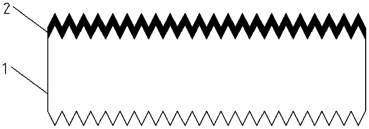
[0073] (2) Use BBr first 3 The gaseous source is used as the ion source for boron diffusion treatment to form the lightly doped region layer 2. The diffusion temperature is 900°C and the diffusion time is 40 minutes. After the diffusion is completed, the square resistance of the N-type crystalline silicon substrate is 120Ω / □, and the surface concentration 8e18cm -3 ; and then wash. Complete the battery structure of this step as figure 2 shown.

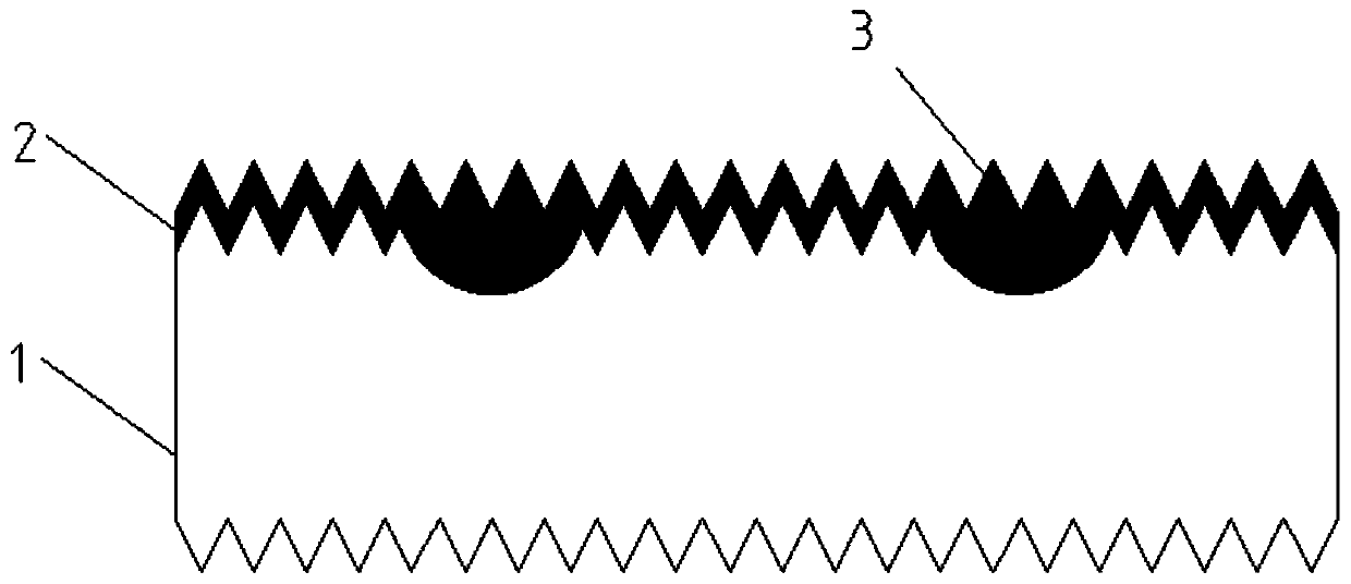
[0074] (3) Through a mask, borane is used as the dopant source of ion implantation on the lightly doped region layer 2 t...

Embodiment 2

[0081] (1) Take an N-type crystalline silicon substrate 1 with a resistivity of 0.3Ω·cm and a thickness of 80 μm, and place the N-type crystalline silicon substrate 1 with a resistivity of 0.3Ω·cm and a thickness of 160 μm in an alkaline solution, A textured surface can be formed on both the back surface and the front surface of the N-type crystalline silicon substrate 1 . Complete the battery structure of this step as figure 1 shown.

[0082] (2) Use BBr first 3 The gaseous source is used as the ion source to carry out boron diffusion treatment to form the lightly doped region layer 2. The diffusion temperature is 1000°C and the diffusion time is 30 minutes. After the diffusion is completed, the square resistance of the N-type crystalline silicon substrate is 150Ω / □, and the surface concentration 5e18cm -3 . Complete the battery structure of this step as figure 2 shown.

[0083] (3) Through a mask, boron fluoride is used as the dopant source of ion implantation on the ...


PUM

PropertyMeasurementUnit
electrical resistivityaaaaaaaaaa
thicknessaaaaaaaaaa
thicknessaaaaaaaaaa

Abstract

The invention relates to a passivation contact solar cell with a selective emitter structure and a preparation method of the passivation contact solar cell. The method comprises the following steps: (1) preparing texturing surfaces on two surfaces of an N-type crystalline silicon substrate; (2) performing boron diffusion treatment on the texturing surface of the front surface of the substrate to form a lightly doped region layer; (3) performing local boron ion implantation on the lightly doped region layer by using a mask, and annealing to form a local heavily doped region; (4) preparing a tunneling oxide layer on the texturing surface of the back surface of the substrate, and preparing a phosphorus-doped polycrystalline silicon layer on the tunneling oxide layer; (5) preparing a silicon nitride antireflection layer on the phosphorus-doped polycrystalline silicon layer; preparing an aluminum oxide passivation layer on the lightly doped region layer on the front surface of the substrate, and preparing a silicon nitride antireflection layer on the aluminum oxide passivation layer; and (6) carrying out silk-screen printing of metallized slurry on the two surfaces of the substrate, andsintering. According to the invention, the composite current on the surface of the emitter can be remarkably reduced, so that the efficiency of the N-type passivation contact battery can be improvedby more than 0.2%.

Description

technical field [0001] The invention relates to the technical field of solar cells, in particular to a passivated contact solar cell with a selective emitter structure and a preparation method thereof. Background technique [0002] The N-type battery uses N-type silicon as the substrate material, which has good resistance to metal impurity pollution and long minority carrier diffusion length. Compared with the traditional p-type battery, it has the advantages of no light-induced attenuation and higher battery efficiency. favored by the market. N-type passivated contact battery is a new type of N-type battery structure. Its tunneling passivation layer provides good surface passivation for the n+ surface, greatly reduces metal contact recombination, and improves the open circuit voltage and short circuit current of the battery. The cell efficiency of this structure is much higher than that of traditional crystalline silicon cell products, which is more conducive to reducing t...

Claims


Application Information

Patent Timeline
Patent Type & Authority Applications(China)
IPC IPC(8): H01L31/18H01L31/068
CPCH01L31/068H01L31/1804Y02E10/546Y02E10/547Y02P70/50
Inventor 陆俊宇季根华陈嘉林建伟
Owner TAIZHOU ZHONGLAI PHOTOELECTRIC TECH CO LTD
Why Eureka
Try Eureka