Method for removing front polycrystalline silicon winding plating

A technology of polycrystalline silicon and polycrystalline silicon layer, applied in the field of solar cells, can solve the problems of increasing process cost, narrow process window, increasing machine equipment, etc., and achieve the effect of reducing production cost, increasing reaction window, and meeting mass production requirements.

Active Publication Date: 2020-06-26
TAIZHOU ZHONGLAI PHOTOELECTRIC TECH CO LTD
View PDF6 Cites 15 Cited by
  • Summary
  • Abstract
  • Description
  • Claims
  • Application Information

AI Technical Summary

Problems solved by technology

[0004] 1) There is a color difference between the wrapping plating area and the non-wrapping plating area, and there is obvious color difference after coating, resulting in poor appearance of the battery;
[0005] 2) The polysilicon in the surrounding plating area has strong light absorption ability, which is not conducive to the absorption of light by the battery, resulting in a decrease in efficiency;
[0006] 3) The polysilicon in the surrounding plating area affects the burn-through effect of the slurry, resulting in a decrease in the fill factor of the battery and a decrease in efficiency;
[0007] 4) The passivation effect of the surrounding plating area is not good, and the surrounding plating area is black, which affects the yield of the cell
[0009] 1. Use HF and HNO 3 The mixed acid system removes the polysilicon coated on the front side of the silicon wafer. This method requires the use of pure HF and HNO 3 Mixed acid, after cleaning 80,000 cells, the cleaning effect will become worse, and the product yield will drop sharply. If more cells need to be cleaned, the solution needs to be replaced, and the cost is high
[0010] 2. Use inorganic alkali (potassium hydroxide or sodium hydroxide) to remove the polysilicon on the front side of the silicon wafer. The solution reaction rate of this method is too fast to control the removal effect. The requirements for the incoming material are very high, and the chemicals are easy to Destroy the p+ layer, the process window is very narrow, and the efficiency and yield fluctuate greatly during mass production
[0011] 3. Use SiO 2 or SiN X To make a mask, this method needs to add two process steps-plating mask and cleaning after the mask, which needs to increase the machine equipment and increase the process cost
[0012] 4. Using the phosphosilicate glass layer as a mask puts forward extremely high requirements on the etching process. During the etching process, it is difficult to completely retain the phosphosilicate glass layer on the front edge of the silicon wafer. If the phosphosilicate glass layer on the edge of the silicon wafer If it is not well preserved, it will not act as a barrier layer in the subsequent process of removing polysilicon plating with alkaline solution, so that the problem of battery leakage cannot be controlled

Method used


Image

  • Method for removing front polycrystalline silicon winding plating
  • Method for removing front polycrystalline silicon winding plating
  • Method for removing front polycrystalline silicon winding plating

Examples


Embodiment 1

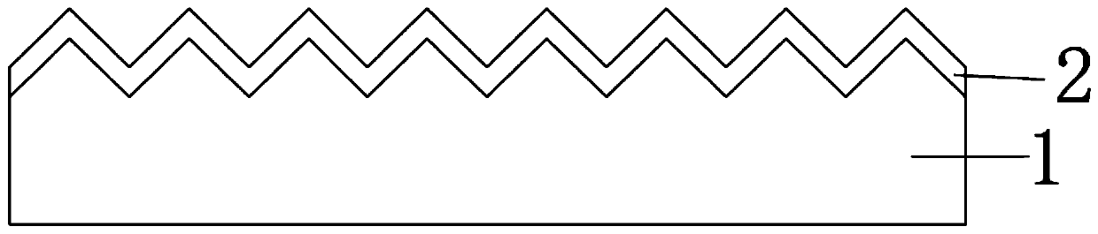
[0076] (1) Take a silicon substrate 1 with a resistivity of 1Ω·cm and a thickness of 160 μm, and place the silicon substrate 1 with a resistivity of 1Ω·cm and a thickness of 160 μm in an alkaline solution, so that the back surface and the front surface of the silicon substrate 1 The surface is made of suede.

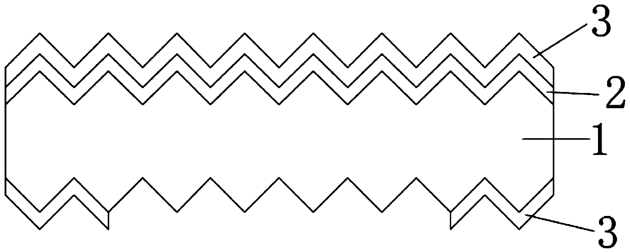
[0077] (2) Boron diffusion is carried out on the front side of the silicon wafer after alkali texturing to form the p+ emitter 2 and the front borosilicate glass layer 3 on the front side of the silicon wafer; during the boron diffusion process, part of the boron atoms diffuse to the back edge of the silicon substrate 1 area, and form the back borosilicate glass layer 3 in the edge area. Complete the battery structure of this step as figure 1 shown.

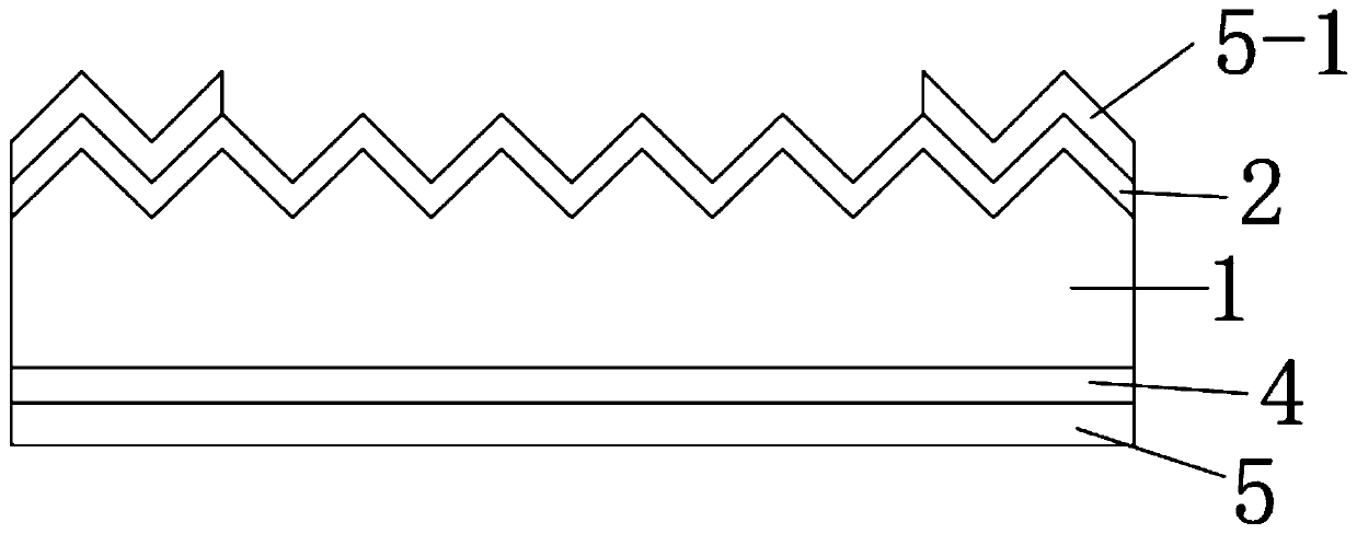
[0078] (3) Place the backside of the silicon wafer treated in step (2) in a mixed acid system of hydrofluoric acid and nitric acid for wet etching. The textured surface on the back of the silicon wafer is etched into a p...

Embodiment 2

[0088] (1) Take a silicon substrate 1 with a resistivity of 0.3Ω·cm and a thickness of 90 μm, and place the silicon substrate 1 with a resistivity of 0.3Ω·cm and a thickness of 90 μm in an alkaline solution, so that on the back of the silicon substrate 1 Both the surface and the front surface form a textured surface.

[0089] (2) Boron diffusion is carried out on the front side of the silicon wafer after alkali texturing to form the p+ emitter 2 and the front borosilicate glass layer 3 on the front side of the silicon wafer; during the boron diffusion process, part of the boron atoms diffuse to the back edge of the silicon substrate 1 area, and form the back borosilicate glass layer 3 in the edge area. Complete the battery structure of this step as figure 1 shown.

[0090] (3) Place the backside of the silicon wafer treated in step (2) in a mixed acid system of hydrofluoric acid and nitric acid for wet etching. The textured surface on the back of the silicon wafer is etched...

Embodiment 3

[0100] (1) Take a silicon substrate 1 with a resistivity of 10Ω·cm and a thickness of 300 μm, and place the silicon substrate 1 with a resistivity of 10Ω·cm and a thickness of 300 μm in an alkaline solution, so that on the back surface and the front surface of the silicon substrate 1 The surface is made of suede.

[0101] (2) Boron diffusion is carried out on the front side of the silicon wafer after alkali texturing to form the p+ emitter 2 and the front borosilicate glass layer 3 on the front side of the silicon wafer; during the boron diffusion process, part of the boron atoms diffuse to the back edge of the silicon substrate 1 area, and form the back borosilicate glass layer 3 in the edge area. Complete the battery structure of this step as figure 1 shown.

[0102] (3) Place the backside of the silicon wafer treated in step (2) in a mixed acid system of hydrofluoric acid and nitric acid for wet etching. The textured surface on the back of the silicon wafer is etched int...


PUM

PropertyMeasurementUnit
electrical resistivityaaaaaaaaaa
thicknessaaaaaaaaaa
thicknessaaaaaaaaaa

Abstract

The invention relates to a method for removing front polycrystalline silicon winding plating. The method comprises the following steps: (1) performing boron diffusion on the front surface of a siliconwafer to form a p + emitter and a front borosilicate glass layer; (2) etching the back surface of the silicon wafer, etching the back surface into a plane, removing the boron-doped layer and the borosilicate glass layer on the back surface and the periphery, and removing the front borosilicate glass layer; (3) growing a tunneling oxide layer and an intrinsic amorphous silicon layer on the back surface of the silicon wafer, and forming a front winding polycrystalline silicon layer on the edge region of the front surface of the silicon wafer; (4) carrying out ion implantation on the intrinsic amorphous silicon layer to form a phosphorosilicate glass layer, and performing annealing to form a phosphorus-doped polycrystalline silicon layer; (5) plating a silicon nitride layer on the phosphorus-doped polycrystalline silicon layer; (6) placing the silicon wafer in a mixed solution of alkali and a single crystal additive to remove the front winding polycrystalline silicon layer; and (7) plating aluminum oxide layers on the two sides of the silicon wafer, and plating a passivation antireflection film layer on the aluminum oxide layer on the front side. According to the method, the reactionrate of the alkali liquor in the alkali winding plating solution and the winding plating polycrystalline silicon can be well controlled, and reaction windows can be increased.

Description

technical field [0001] The invention relates to the technical field of solar cells, in particular to a method for removing polysilicon wrapping on the front side. Background technique [0002] In crystalline silicon solar cells, serious recombination exists in the metal-semiconductor contact region, which becomes an important factor restricting the development of crystalline silicon solar cell efficiency. The tunnel oxide passivation metal contact structure is composed of an ultra-thin tunnel oxide layer and doped polysilicon layer, which can significantly reduce the recombination of the metal contact area, and at the same time have good contact performance, which can greatly improve the efficiency of solar cells. In order to evaluate the efficiency potential of current commercial high-efficiency cells, such as PERC, HIT, passivated contact cells, etc., the well-known German Institute for Solar Energy Research (ISFH) theoretically based on the concept of carrier selectivity ...

Claims


Application Information

Patent Timeline
Patent Type & Authority Applications(China)
IPC IPC(8): H01L31/18H01L31/068
CPCH01L31/068H01L31/1804Y02E10/546Y02P70/50
Inventor 陈嘉展士飞陈程邱军辉陆佳刘志锋林建伟
Owner TAIZHOU ZHONGLAI PHOTOELECTRIC TECH CO LTD
Why Eureka
Try Eureka