Indium column of infrared focal plane detector and preparation method thereof

An infrared focal plane and detector technology, which is applied in the field of infrared detectors, can solve the problems of poor chip unevenness compensation ability, poor uniformity of indium column size, and deterioration, so as to achieve uniform and smooth surface of indium column, The effect of improving the uniformity of indium column size and high controllability of the process

Active Publication Date: 2020-08-25
武汉华中旷腾光学科技有限公司
View PDF7 Cites 7 Cited by
  • Summary
  • Abstract
  • Description
  • Claims
  • Application Information

AI Technical Summary

Problems solved by technology

[0004] With the continuous increase of detector array size and imaging resolution on the application side, the distance between the center of the pixel is continuously reduced. In order to avoid the short circuit between the pixels due to the deformation of the indium column, the lateral dimension of the indium column is required to be reduced accordingly, resulting in direct growth. A sharp drop in the height of the obtained indium column
There are two problems: 1) As the height of the indium column decreases, the leveling tolerance of the chip interconnection decreases, and the slight leveling deviation during the interconnection will cause the interconnection failure of some areas on the side of the sensitive element, and the unevenness of the chip 2) The ability to alleviate the shear deformation caused by the thermal mismatch between the sensitive chip and the readout circuit chip deteriorates, the reliability of the device's thermal shock resistance decreases, and the fatigue life reduce
However, the existing traditional method to increase the height of the indium column usually adopts the thick glue photolithography process, but the thick glue process will lead to the deterioration of the size uniformity of the indium column, and with the increase of the area array density, the thick glue peeling becomes more difficult

Method used


Image

  • Indium column of infrared focal plane detector and preparation method thereof
  • Indium column of infrared focal plane detector and preparation method thereof
  • Indium column of infrared focal plane detector and preparation method thereof

Examples


preparation example Construction

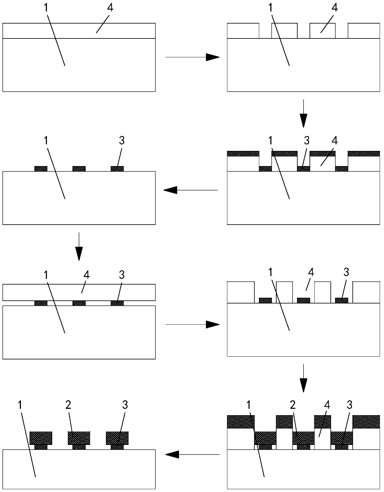
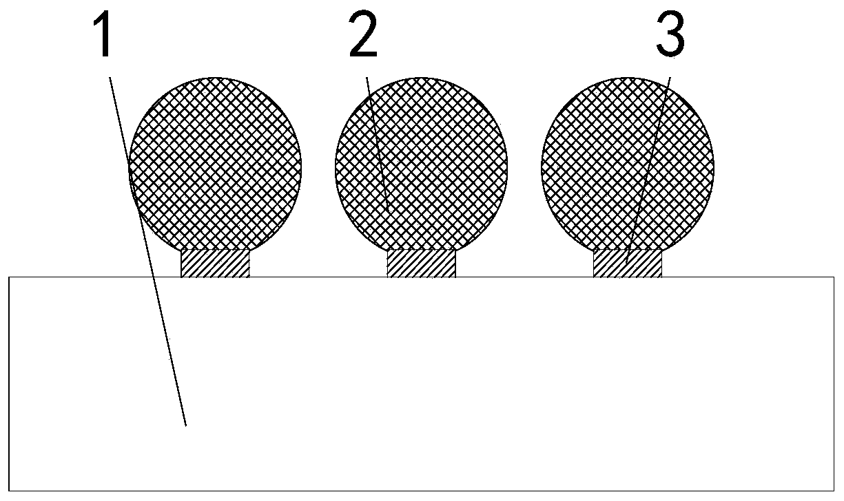
[0031] Such as figure 1 Shown, the preparation method of the indium column of a kind of infrared focal plane detector designed by the present invention comprises the following steps:

[0032] 1) Glue coating on chip 1: clean the surface of chip 1 and remove residual moisture, and then spin-coat a layer of photoresist 4 on the surface of chip 1;

[0033] 2) Mask etching: according to the pitch size parameters of the indium pillars 2, the circular photolithography holes are spaced on the mask plate, and then the mask plate is covered on the chip 1 after step 1) glued, and the first time is carried out. Photolithographic exposure, then developing and fixing;

[0034] 3) Plating the base metal 3: using the vacuum coating method to plate the base metal 3 on the surface of the chip 1 after step 2), and then cleaning off the photoresist 4, and stripping off the excess metal;

[0035] 4) Coating again: Spin-coat a layer of photoresist 4 again on the surface of the chip 1 treated in ...

Embodiment 1

[0052] 1) Chip 1 cleaning: Chip 1 was ultrasonically cleaned with acetone and isopropanol for 3 minutes, and then rinsed with deionized water.

[0053] 2) Coating of chip 1: Spin-coat AZ5214 photoresist 4 on the surface of cleaned chip 1, spin-coat a thin layer of glue with a homogenizer, select the number of rotations to be 4000 rpm, and spin-coat for 30 seconds , After the glue is placed, it needs to be heated at 95 ℃ for 90 seconds.

[0054] 3) Mask etching: according to the pitch size parameters of the indium pillars 2, circular photolithographic holes with a diameter of 5 μm are separated on the mask plate, and then the mask plate is covered on the chip 1 coated with glue, and the first time is carried out. For photolithography exposure, the exposure dose was controlled at 58.2 millijoules per square centimeter.

[0055] 4) Developing and fixing: the exposed chip 1 is put into a developing solution with a concentration of 2.38% tetramethylammonium hydroxide for 55 second...

Embodiment 2

[0065] 1) Chip 1 cleaning: Chip 1 was ultrasonically cleaned with acetone and isopropanol for 3 minutes, and then rinsed with deionized water.

[0066] 2) Coating of chip 1: Spin-coat AZ5214 photoresist 4 on the surface of cleaned chip 1, spin-coat a thin layer of glue with a homogenizer, select the number of rotations to be 4000 rpm, and spin-coat for 30 seconds , After the glue is placed, it needs to be heated at 95 ℃ for 90 seconds.

[0067] 3) Mask etching: according to the pitch size parameters of the indium pillars 2, circular photolithographic holes with a diameter of 6 μm are separated on the mask plate, and then the mask plate is covered on the chip 1 coated with glue, and the first time is carried out. For photolithography exposure, the exposure dose is controlled at 60.5 millijoules per square centimeter.

[0068] 4) Developing and fixing: the exposed chip 1 was put into a developing solution with a concentration of 2.38% tetramethylammonium hydroxide for 45 second...


PUM

PropertyMeasurementUnit
diameteraaaaaaaaaa
sizeaaaaaaaaaa
heightaaaaaaaaaa

Abstract

The invention relates to a preparation method of an indium column of an infrared focal plane detector and the indium column prepared by the method. The method comprises the following steps of spin-coating thin photoresist on the surface of a chip, aligning to the center of a pixel or a reading unit electrode to carry out primary overlay, preparing a circular bottoming metal deposition hole, evaporating a composite metal film through electron beam evaporation, and obtaining a bottoming metal pattern array by adopting a wet stripping mode, secondly, spin-coating photoresist with medium thickness, aligning to the center of the bottoming metal pattern to carry out secondary overlay, preparing a square indium column deposition hole, depositing an indium film through vacuum thermal evaporation,and obtaining an indium column by adopting a wet stripping process, and finally, performing ball shrinkage in a formic acid atmosphere by adopting a reflux furnace to obtain the indium column array with a large height-width ratio. Compared with the prior art, the overall process difficulty is lower, the size of the prepared indium column can meet the requirement, the size uniformity is high, the surface of the indium column is uniform and smooth, and the consistency requirement of the inverted interconnection process can be completely met.

Description

technical field [0001] The invention relates to the technical field of infrared detectors, in particular to an indium column of an infrared focal plane detector and a preparation method thereof. Background technique [0002] The infrared focal plane array (IRFPA) detector has the functions of radiation sensitivity, charge storage and multiplex transmission. The number of detection units of the detector is more than 3 orders of magnitude higher than that of the first-generation detector, and the rapid electronic scanning imaging, identification and tracking of the target are realized through the Flip-Chip process (Flip-Chip) and the CMOS readout circuit technology. , tracking, staring imaging and other weapons and equipment are widely used. In recent years, people have gradually proposed the concept of the third-generation infrared detector with the technical characteristics of high detection rate, large area array, low cost, and multi-spectrum. Based on the second-generatio...

Claims


Application Information

Patent Timeline
Patent Type & Authority Applications(China)
IPC IPC(8): H01L31/101H01L31/0203H01L23/498
CPCH01L31/101H01L31/0203H01L23/49816Y02P70/50
Inventor 齐志强潘德彬孙昊骋胡文良
Owner 武汉华中旷腾光学科技有限公司
Why Eureka
Try Eureka