Construction method of 3D micro/nano structure

A nanostructure and 3D technology, applied in the field of 3D micro/nanostructure construction, can solve problems such as complex structure reverse replication process, and achieve the effect of good application and promotion value

Active Publication Date: 2020-09-11
HENAN UNIVERSITY
View PDF6 Cites 5 Cited by
  • Summary
  • Abstract
  • Description
  • Claims
  • Application Information

AI Technical Summary

Problems solved by technology

To realize metal-oxide-semiconductor devices, a complex structure inversion replication process is also required

Method used


Image

  • Construction method of 3D micro/nano structure
  • Construction method of 3D micro/nano structure
  • Construction method of 3D micro/nano structure

Examples


Embodiment 1

[0026] A method for constructing a 3D micro / nano structure, comprising the following steps:

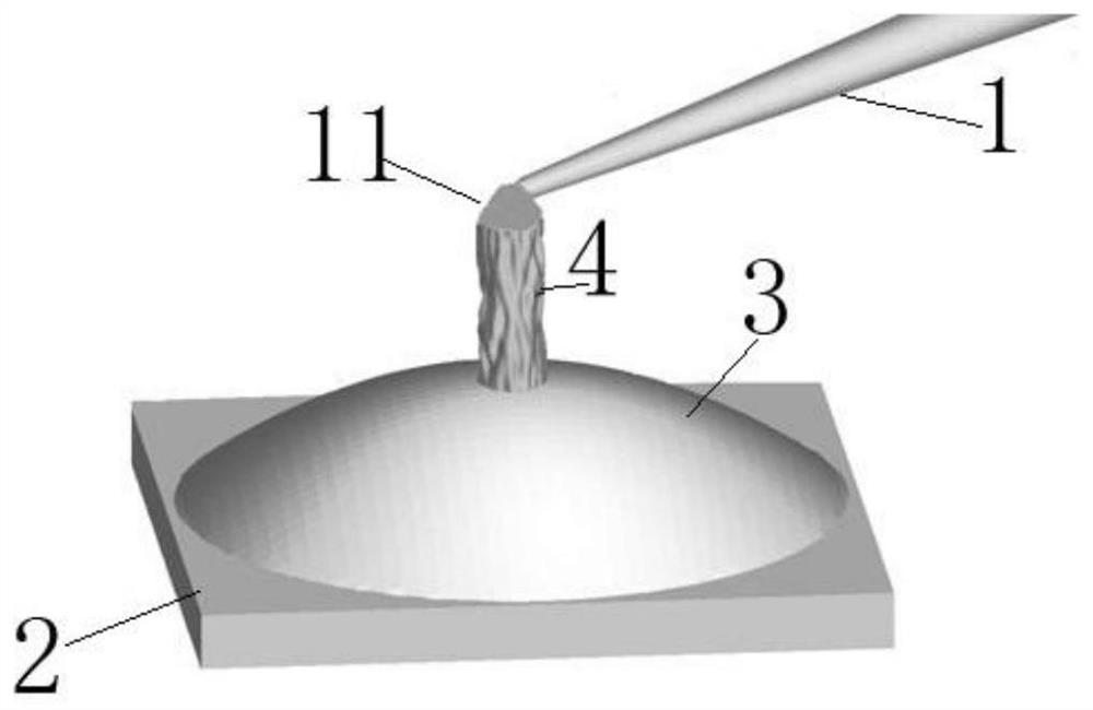
[0027] (1) Take a silicon wafer with a length and width of 1 cm and use ultrapure water, ethanol, and acetone for 10 minutes of ultrasonication as the substrate 2, and deposit a layer of ZnO film with a thickness of 100 nm on the silicon substrate by magnetron sputtering coating method , with this ZnO thin film as the material source for building a three-dimensional structure 3, put the silicon substrate on which the ZnO thin film is deposited into the vacuum chamber of the electron microscope to evacuate, so that the vacuum degree reaches 10 - 4 Pa;

[0028] (2) Turn on the filament, adjust the state of the electron beam 1 and the grating displacement platform, the working distance is 7mm, the accelerating voltage is 10kV, the electron beam spot is 10nm, and the electron beam 1 is obliquely incident on the ZnO surface at an angle of 70° (such as figure 1 shown), the electron beam f...

Embodiment 2

[0031] A method for constructing a 3D micro / nano structure, comprising the following steps:

[0032] (1) Synthesize cobalt-nickel hydroxide polycrystalline nanowires by hydrothermal method, then anneal at 400 degrees Celsius for 2 hours in a muffle furnace to form cobalt-nickel oxide polycrystalline nanowire powders, and disperse cobalt-nickel oxide polycrystalline nanowires into On the silicon wafer substrate, as the source material for growing nano-germ, put the above-mentioned silicon wafer substrate into the vacuum chamber of the electron microscope to evacuate, so that the vacuum degree reaches 10 -3 Pa;

[0033] (2) Turn on the filament, adjust the state of the electron beam and the grating displacement platform, the working distance is 12mm, the accelerating voltage is 15kV, the electron beam spot is 20nm, and the electron beam is focused so that the focus of the electron beam is located at the growth point of the cobalt-nickel oxide polycrystalline nanowire powder The...

Embodiment 3

[0036] A method for constructing a 3D micro / nano structure, comprising the following steps:

[0037] (1) Take a copper sample stage as the substrate, take a section of copper wire, pull it off forcefully, fix it on the copper sample stage with conductive tape, use the broken end of the copper wire as the growth point of the nanorod, and place the copper sample stage above Put it into the electron microscope vacuum chamber to evacuate to make the vacuum degree reach 10 -5 Pa;

[0038](2) Turn on the filament, adjust the state of the electron beam and the grating displacement platform, the working distance is 20mm, the accelerating voltage is 30kV, the beam spot of the electron beam is 50nm, and the electron beam is focused so that the focus of the electron beam is located in the vicinity of the copper wire growth point, and the copper wire grows The distance between the points is 50nm, and the surface layer near the electron beam focus and the copper wire growth point forms a ...


PUM

PropertyMeasurementUnit
diameteraaaaaaaaaa

Abstract

The invention discloses a construction method of a 3D micro / nano structure, which comprises the following steps: (1) fixing a material source on a substrate, and carrying out vacuumizing; (2) focusingthe focus of the electron beam at a place having a distance of 0-100nm away from the surface of the material source in the step (1) to form an interface local area containing the focus of the electron beam and surface layer atoms; and (3) controlling the focus of the electron beam to move point by point according to the designed 3D micro / nano structure to achieve the construction of the 3D micro / nano structure. According to the construction method of the present invention, focusing electron beam focus heat radiation is used for regulating material source surface layer atoms; the surface atomkinetic energy is increased; the constraint of surface energy is overcome, and the atons escape from the surface; and meanwhile, surface layer atoms of a material source are diffused to a low-densityarea due to the imbalance of the atomic density of an interface local area and the potential energy difference, so that the real-time construction of a three-dimensional structure under a micro / nano scale is achieved, the fusion development of a nano technology and 3D printing is promoted, and the application and popularization values are relatively good.

Description

technical field [0001] The invention relates to a method for constructing a nanostructure, in particular to a method for constructing a 3D micro / nanostructure. Background technique [0002] At the micro / nano scale, the movement laws of electrons, photons and phonons of materials are restricted by their microstructure. The confinement effect of this micro / nanostructure makes it have many novel physical and chemical properties. It has broad application prospects in the fields of energy and environment. Therefore, the processing and preparation technology of micro / nanostructure materials has attracted much attention. [0003] In order to achieve precise control over the size, composition and structure of materials, a series of synthetic and preparation methods have been developed. It can be roughly divided into two categories: bottom-up and top-down. Bottom-up methods, such as gas-liquid-solidification vapor deposition, solid-liquid-solid process, and self-assembly methods, ...

Claims


Application Information

Patent Timeline
Patent Type & Authority Applications(China)
IPC IPC(8): B81C1/00B81B7/00
CPCB81C1/00015B81C1/00349B81C1/00436B81B7/00B33Y10/00B22F10/366B22F10/36B22F10/20B33Y50/02B22F2999/00B82Y30/00Y02P10/25B22F1/0547B22F1/068B22F2201/20B33Y70/00B22F12/41B22F12/70B22F2302/25B81C1/00373B81C1/00626B81C2201/0183B82Y40/00
Inventor 杨光红贾彩虹
Owner HENAN UNIVERSITY
Why Eureka
Try Eureka