Copper-indium-gallium-selenium thin-film solar cell module and preparation method thereof

A solar cell, copper indium gallium selenide technology, applied in electrical components, circuits, photovoltaic power generation, etc., can solve the problems of residue falling into the trench, affecting photoelectric conversion efficiency, and high equipment cost, so as to reduce the possibility of leakage current performance, improve photoelectric conversion efficiency, and improve process compatibility

Active Publication Date: 2020-12-25
CHINA TRIUMPH INT ENG
View PDF6 Cites 0 Cited by
  • Summary
  • Abstract
  • Description
  • Claims
  • Application Information

AI Technical Summary

Problems solved by technology

Although the mechanical scribing method is simple and direct, the large line width leads to a large dead zone, which affects the photoelectric conversion efficiency; the edge chipping phenomenon is serious, and the residue falls into the groove, which may cause a short circuit; the mechanical needle directly contacts the film layer, causing wear and tear. Large, it needs to be shut down for replacement every few days, which seriously affects production; at the same time, the laser equipment for marking processes in different processes is far away from each other, and cannot be processed in a centralized manner. The cost of equipment is high, the error is large, and the efficiency is low

Method used


Image

  • Copper-indium-gallium-selenium thin-film solar cell module and preparation method thereof
  • Copper-indium-gallium-selenium thin-film solar cell module and preparation method thereof
  • Copper-indium-gallium-selenium thin-film solar cell module and preparation method thereof

Examples


Embodiment 1

[0056]This embodiment provides a method for preparing a copper indium gallium selenide solar cell module, which uses picosecond infrared lasers to realize the P2 / P3 (second slit and third slit) process scribing of the copper indium gallium selenide module. The picosecond infrared laser pulse has a very high energy intensity and a very high power density, which is enough to strip the outer layer of the material and achieve the effect of removing the "electronic state" of the material. It has high efficiency, no thermal effect and a non-contact process, so there is no edge chipping. There are no cracks and residual stress. The scribing quality fully meets the process requirements of CIGS module production for CIGS thin-film solar scribing, greatly improving the scribing quality. In addition, the line width of picosecond infrared laser scribing is very small, which is effective Reduce the dead zone area of ​​the battery module and improve the photoelectric conversion efficiency of the ...

Embodiment 2

[0079]This embodiment provides a copper indium gallium selenide thin-film solar cell module. The copper indium gallium selenide thin-film solar cell module can be prepared by the preparation method of the first embodiment, but is not limited to the preparation method described in the first embodiment, as long as it can be formed This copper indium gallium selenium thin film solar cell module is sufficient. The beneficial effects that can be achieved by the copper indium gallium selenide thin film solar cell module can be found in the first embodiment, which will not be described in detail below.

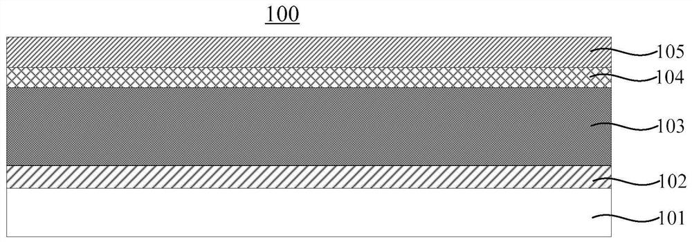
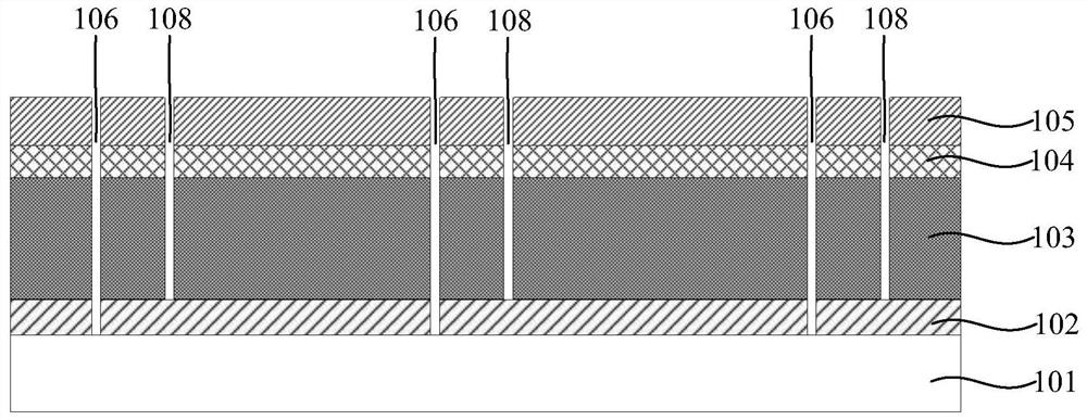
[0080]Such asFigure 2 to Figure 7As shown, the copper indium gallium selenium thin film solar cell module includes:

[0081]At least two battery blocks 115 formed on the copper indium gallium selenide solar cell film 100. The copper indium gallium selenide solar cell film 100 includes a substrate 101, a back electrode layer 102, a copper indium gallium selenide absorption layer 103, The buffer l...


PUM

PropertyMeasurementUnit
widthaaaaaaaaaa
widthaaaaaaaaaa
thicknessaaaaaaaaaa

Abstract

The invention provides a copper-indium-gallium-selenium thin-film solar cell module and a preparation method thereof. The method comprises the following steps: providing a copper-indium-gallium-selenium solar cell thin film; etching the battery film at an etching depth which is stopped on the upper surface of the substrate to form a first etching seam; etching the cell film by using picosecond infrared laser, and stopping etching depth on the upper surface of the back electrode layer to form a third etching seam; performing insulating material coating on the first carving seam and the third carving seam; using picosecond infrared laser to scribe the cell film, stopping the scribing depth on the upper surface of the back electrode layer, and forming a second scribing seam between the firstscribing seam and the third scribing seam; and performing conducting material coating on the second carving seam. Through one-stop centralized laser scribing treatment, the equipment error is small, the process window is large, a coating process does not need to be adjusted to adapt to a scribing process, and the process compatibility is improved; burrs or surface residual chippings are avoided, and the hidden danger of battery short circuit is eliminated; and the notch line width is small, the dead zone area is reduced, and the conversion efficiency of the battery assembly is improved.

Description

Technical field[0001]The present invention relates to the technical field of thin film solar cells, and in particular to a copper indium gallium selenium thin film solar cell component and a preparation method thereof.Background technique[0002]With the increasing energy crisis and environmental pollution, how to increase the proportion of renewable energy and adjust the energy structure has become the mainstream of social development. As an important renewable energy source, solar energy has received extensive attention in recent years and has developed rapidly.[0003]Copper Indium Gallium Selenide (CuInGaSe2, Referred to as CIGS) thin-film solar cell is a device that can convert light energy into electrical energy. Its basic structure includes p-type CIGS and n-type CdS / In2S3The PN heterojunction formed after semiconductor materials contact each other, where the direction of the built-in electric field of the PN junction is from the n-type semiconductor to the p-type semiconductor. ...

Claims


Application Information

Patent Timeline
Patent Type & Authority Applications(China)
IPC IPC(8): H01L31/18H01L31/0463H01L31/0749
CPCH01L31/0749H01L31/18H01L31/1876H01L31/0463Y02E10/541Y02P70/50
Inventor 彭寿殷新建陈瑛周显华钱双
Owner CHINA TRIUMPH INT ENG
Why Eureka
Try Eureka