Composite gradient laminated solder preform for power electronics and manufacturing method thereof

A solder preform and power electronics technology, which is applied in the field of power electronics, can solve problems such as poor mechanical properties, low reliability, and large amount of precious metals, and achieve excellent electrical and thermal conductivity, high temperature resistance and reliability, and simple preparation methods. Effect

Active Publication Date: 2022-01-18
INST OF ELECTRICAL ENG CHINESE ACAD OF SCI
View PDF12 Cites 0 Cited by
  • Summary
  • Abstract
  • Description
  • Claims
  • Application Information

AI Technical Summary

Problems solved by technology

The thickness of the welding layer using this welding technology is generally less than 20 μm, which is not conducive to absorbing the thermal stress caused by the adaptation of the thermal expansion coefficient of system materials such as chips and substrates, and it is difficult to meet the needs of high-reliability packaging of power electronic devices
Chinese patent CN100475996C discloses a composition, production method and components for high-temperature lead-free solder. The phase line is not lower than 262.5°C, and the liquidus line is not higher than 400°C. However, the strength and plasticity of the lead-free solder composition are low, and the solder paste made of ordinary solder paste for this solder has poor collapse resistance. , more tin beads and other defects are unfavorable for the industrialized production and promotion of the composition for lead-free solder
The amount of precious metals is large, the cost is high, and the welding temperature is high; Chinese patent CN104588906 A discloses a Sn-Cu high-temperature lead-free solder paste and its preparation method and use method. High shear strength and stable performance, but this technology still uses solder paste, which requires a screen printing process that is prone to pollution; due to the welding process, the solder material cannot be wetted and spread, so a large area is left after the solder paste volatilizes Holes and loose joints affect thermal conductivity and reliability; Chinese patent CN103753049A discloses a Cu / Sn composite solder preform, although it solves the problem of large voids caused by volatilization of solder paste, it still has poor toughness and strong toughness. The problem of mismatch, at the same time, there is non-coplanarity with the chip and the substrate, and the interface is difficult to achieve dense welding, resulting in large contact thermal resistance, poor mechanical properties, and low reliability.

Method used


Image

  • Composite gradient laminated solder preform for power electronics and manufacturing method thereof
  • Composite gradient laminated solder preform for power electronics and manufacturing method thereof
  • Composite gradient laminated solder preform for power electronics and manufacturing method thereof

Examples


Embodiment 1

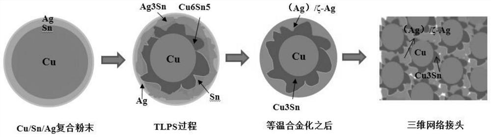
[0039] Copper powder with a particle size of 5-10 μm and 10-15 μm is used to prepare the electroplating Sn coating and the physical vapor deposition Ag coating respectively, and the particle size is graded according to the ratio of 3:2, and the graded powder is placed in a high-speed ball mill. , mechanically mixed at a rate of 100r / min for 1h to obtain a homogeneously mixed composite powder.

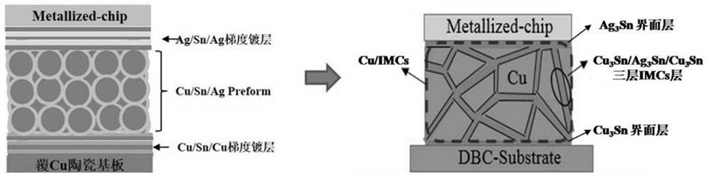
[0040] Weigh 0.13 g of the above-mentioned mixed powder, perform high-pressure tablet pressing on a press with a pressure of 10 MPa, and hold a constant pressure for 10 minutes to obtain a solder sheet with a thickness of 345 μm. Prepare the compound gradient coating on the upper and lower surfaces of the preform prepared above by magnetron sputtering. One side of the welding chip is a repeating structural unit of "Ag / Sn / Ag", and the side of the welding substrate is "Cu / Sn / Cu "Repeating structural units, the thickness of each structural unit gradually increases from the Preform to the d...

Embodiment 2

[0044] Copper powders with a particle size of 5-10 μm and 15-20 μm were used for electroplating Sn and sputtering Ag coatings respectively, and the particle size was graded according to the ratio of 3:1, and the graded powder was placed in a high-speed ball mill. Mix mechanically for 2 hours at a rate of 200r / min to obtain a uniformly mixed composite powder.

[0045] Weigh 0.13 g of the above-mentioned mixed powder, perform high-pressure tablet pressing on a press with a pressure of 15 MPa, and hold a constant pressure for 10 minutes to obtain a solder sheet with a thickness of 300 μm. The preform Preform prepared above was prepared by magnetron sputtering to prepare the upper and lower surface gradient composite laminated structures as "Ag / Sn / Ag"g and "Cu / Sn / Cu" respectively, and the thickness of the innermost structural unit is 600nm. The increasing thickness gradient is 120 nm, the number of repeating structural units is 10, and the total thickness is 14 μm.

[0046] The s...

Embodiment 3

[0048] Copper powders with a particle size of 5-15 μm and 15-30 μm were used for electroplating Sn and sputtering Ag coatings respectively, and the particle size was graded according to the ratio of 3:1. The graded powder was placed in a high-speed ball mill. Mix mechanically for 1 hour at a rate of 500 r / min to obtain a uniformly mixed composite powder.

[0049] Weigh 0.13 g of the above-mentioned mixed powder, perform high-pressure tablet pressing on a press with a pressure of 10 MPa, and hold a constant pressure for 5 minutes to obtain a solder sheet with a thickness of 200 μm. The Preform prepared above was prepared by magnetron sputtering to prepare the upper and lower surface gradient composite coating structures as "Ag / Sn / Ag" and "Cu / Sn / Cu" respectively, the innermost structural unit thickness is 500nm, and the incremental thickness gradient is 150nm. The number of repeating structural units is 12, and the total thickness is 15 μm.

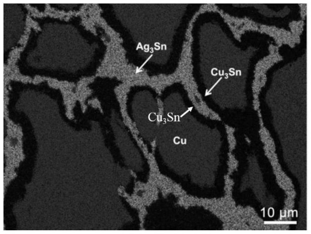
[0050] Sinter the solder preform wi...


PUM

PropertyMeasurementUnit
thicknessaaaaaaaaaa
thicknessaaaaaaaaaa
thicknessaaaaaaaaaa

Abstract

The invention relates to a composite gradient laminated solder preform for power electronics and a manufacturing method thereof, comprising: a composite preform body, the body is formed by pressing Cu / Sn / Ag core-shell powder; the Cu / Sn / Ag core-shell structure powder is prepared by electroplating Sn on Cu powder with different particle sizes to prepare Cu / Sn powder, and then sputtering and plating Ag on Cu / Sn powder to obtain Cu / Sn / Ag powder; the surface of the body is made of Multi-layer composite gradient lamination, the thickness of each layer of composite gradient lamination gradually increases from the inside to the outside; the multi-layer composite gradient lamination adopts the physical vapor deposition process to carry out the first melting point and the second melting point respectively on the upper and lower surfaces of the body. Alternate metal sputtering coating treatment to complete the preparation, the temperature of the first melting point is higher than the second melting point. The present invention prepares gradient multi-layer coatings on the surface of the preformed soldering sheet, and at the same time electroplates a Sn layer on the surface of the copper-clad ceramic substrate (DBC). Soldered joints with thermal resistance and high mechanical reliability.

Description

technical field [0001] The invention relates to the field of power electronics, in particular to a composite gradient laminated preform for power electronics and a manufacturing method thereof. Background technique [0002] Power electronic modules are used more and more widely in electric vehicles, aerospace, rail transit, etc. The third-generation wide-bandgap semiconductors such as SiC, because of their high melting point, high power density, and superior thermal and electrical conductivity, have become the best materials to replace Si chips. To give full play to the superior performance of SiC chips, high-temperature-resistant chip soldering materials and soldering Technology is the key and constraint. [0003] Traditional high temperature soldering materials include Au-Sn, Bi-Ag-xSn-xPb, Sn-Pb-Ag. Due to the high cost of Au and Ag precious metals, the soldering temperature is 280-330°C, which affects the performance of temperature-sensitive components; with the promul...

Claims


Application Information

Patent Timeline
Patent Type & Authority Patents(China)
IPC IPC(8): B23K20/00B23K35/00B23K35/40B22F1/17C23C28/02
CPCB23K35/40B23K35/00B23K20/00C23C28/023B22F1/17
Inventor 徐红艳徐菊
Owner INST OF ELECTRICAL ENG CHINESE ACAD OF SCI
Why Eureka
Try Eureka