Method for manufacturing a structural color filter

A technology of optical filter and structural color, applied in the direction of optical filter, optics, optical components, etc., can solve problems such as limiting application scenarios, increasing process complexity and difficulty, and complex processing technology

Pending Publication Date: 2021-01-08
NINGBO INLIGHT TECH CO LTD +1
View PDF2 Cites 0 Cited by
  • Summary
  • Abstract
  • Description
  • Claims
  • Application Information

AI Technical Summary

Problems solved by technology

[0005] The processing technology of structural color devices using plasma structure or guided mode resonance structure is complicated, and usually requires expensive and time-consuming processing methods such as electron beam etching and focused ion beam etching, which cannot be applied in large areas.
The three-dimensional photonic crystal structure formed by the nanoparticle self-assembly process is a potential solution to realize the large-area and low-cost application of structural color, but this technology has very high requirements for the flatness and smoothness of the substrate. Limits its application scenarios
Considering that the processing of structural color devices mostly requires vacuum equipment and high temperature conditions to ensure the optical quality of the film material, this additionally increases the complexity and difficulty of the process

Method used


Image

  • Method for manufacturing a structural color filter
  • Method for manufacturing a structural color filter
  • Method for manufacturing a structural color filter

Examples


Embodiment 1

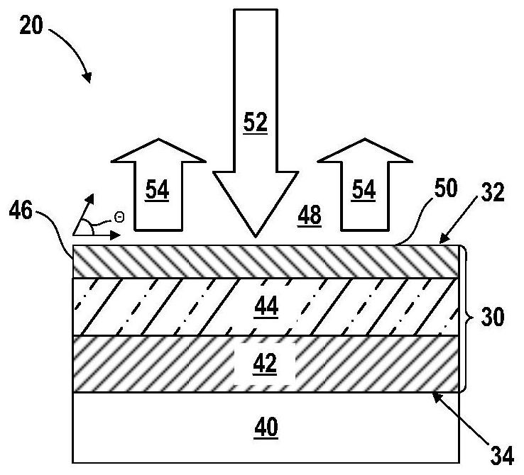
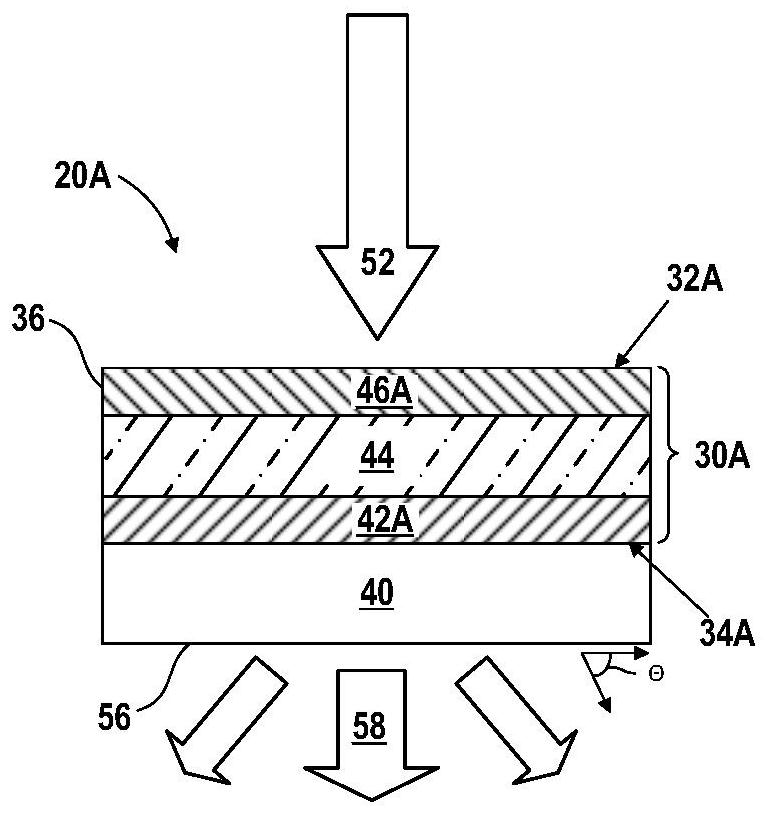
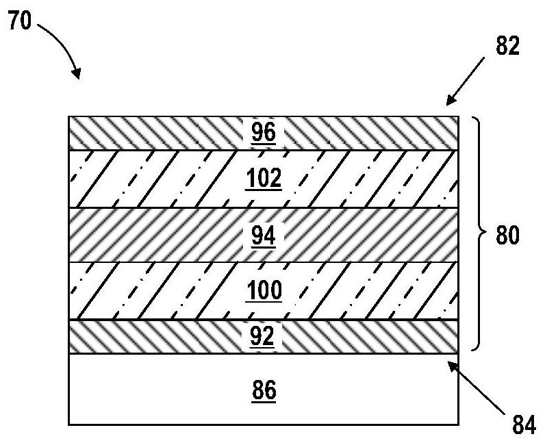
[0107] attached Figure 5A It is a schematic diagram of a structural color filter device processed according to the solution method described in the present invention, as shown in the figure, it is formed by sequentially electroplating Au / Cu on a crystalline silicon (Si) substrate 2 O / Au three-layer film (MDM stacked film).

[0108] The following raw materials were used in processing: acetone (ACS grade, Fisher Scientific), methanol (ACS grade, Fisher Scientific), isopropanol (ACS grade, Fisher Scientific), buffered hydrofluoric acid (BHF) (Transene Inc.), hydrofluoric acid acid (HF) (49%, Transene Inc.), gold(III) chloride trihydrate (HAuCl 4 3H2O) (>99.9%, Sigma-Aldrich), potassium sulfate (K 2 SO 4 ) (ACS grade, Fisher Scientific), potassium chloride (KCl) (ACS grade, Fisher Scientific), sulfuric acid (H 2 SO 4 ) (0.1M concentrate for IC, Sigma-Aldrich), copper(II) sulfate pentahydrate (CuSO 4 ·5H 2 O) (ACS grade, Avantor), citric acid (>99.5% ACS grade, Sigma-Aldric...


PUM

PropertyMeasurementUnit
Thicknessaaaaaaaaaa
Thicknessaaaaaaaaaa
Thicknessaaaaaaaaaa

Abstract

A method of manufacturing a structural color filter includes: contacting a substrate with a first electrolyte; applying a voltage to the substrate so as to enable the first metal layer to be depositedon a substrate; wherein the first electrolyte contains a first precursor material, the voltage initiates an electrochemical reaction of the first precursor material, a product of the electrochemicalreaction is deposited on the surface of the substrate to form the first metal layer, and the temperature of the deposition process is less than or equal to 50 DEG C; contacting the first metal layer with a second electrolyte to deposit a first dielectric layer on the first metal layer, wherein the second electrolyte contains a second precursor material; and depositing a second metal layer on the first dielectric layer, so that the first metal layer and the second metal layer are positioned on two opposite sides of the dielectric layer. According to the method disclosed in the invention, the deposition is carried out under natural conditions, and the common film deposition of the metal layer, the dielectric layer and the substrate can be realized regardless of the roughness and the curved surface degree of the substrate. According to the method, the process utilizing the three-electrode electrochemical device can be used for controlling and detecting the film forming process, the deposition rate and the film thickness of the film layer.

Description

[0001] This application claims priority to U.S. Provisional Application No. 62 / 852,488, filed May 24, 2019, which is incorporated herein in its entirety. technical field [0002] The present application relates to the field of displays, in particular to a method for preparing a structural color filter. Background technique [0003] Color filters are one of the important components in the field of display, and they are used in various technologies such as flat panel display, liquid crystal display, projection display, wearable display, light emitting diodes (LEDs), complementary metal oxide semiconductor (CMOS) image sensors, etc. important role. For example, transmissive color filters are widely used in liquid crystal displays. Traditional color filters use chemical pigments to absorb the complementary colors of the three primary colors of red, green and blue to produce the three primary colors of red, green and blue. These chemical pigments have various deficiencies, such...

Claims


Application Information

Patent Timeline
IPC IPC(8): G02B5/28
CPCG02B5/28G02B5/288G02B5/286G02B5/20G02F1/133516H01L27/14621H10K59/12
Inventor 季陈纲郭凌杰所罗伯·阿查里雅斯蒂芬·马尔多纳多
Owner NINGBO INLIGHT TECH CO LTD
Why Eureka
Try Eureka