
Reusable Raman enhanced substrate as well as preparation method and application thereof

A substrate, Raman technology, applied in Raman scattering, nanotechnology for sensing, nanotechnology for materials and surface science, etc., can solve the problem of uniformity affecting SERS substrate quality, nanoparticle uniformity, Reduce hot spot density and other issues to achieve the effect of improving SERS performance, photocatalytic performance, and optical performance

Active Publication Date: 2021-03-02
SOUTH CHINA NORMAL UNIVERSITY
View PDF4 Cites 0 Cited by
  • Summary
  • Abstract
  • Description
  • Claims
  • Application Information

AI Technical Summary

Problems solved by technology

However, although these physical methods greatly improve the preparation efficiency of the substrate, the uniformity of the particles greatly affects the quality of the SERS substrate.
At the same time, due to the limitations imposed by the technology, these physical methods lead to the accumulation of nanoparticles in the vertical direction, so that the "hot spot" area between the nanoparticles is covered, thereby reducing the hot spot density on the entire substrate.
In addition, the disadvantages of physical methods such as high cost, harsh experimental conditions, and easy damage to the array structure have also brought great challenges to the development of the experiment.
It can be seen that there are three main problems in the construction process of the three-dimensional SERS substrate: 1. The uniformity of nanoparticles; 2. The density of hot spots caused by the accumulation of nanoparticles; 3. The limitation of experimental conditions

Method used


Image

  • Reusable Raman enhanced substrate as well as preparation method and application thereof
  • Reusable Raman enhanced substrate as well as preparation method and application thereof
  • Reusable Raman enhanced substrate as well as preparation method and application thereof

Examples


Embodiment 1

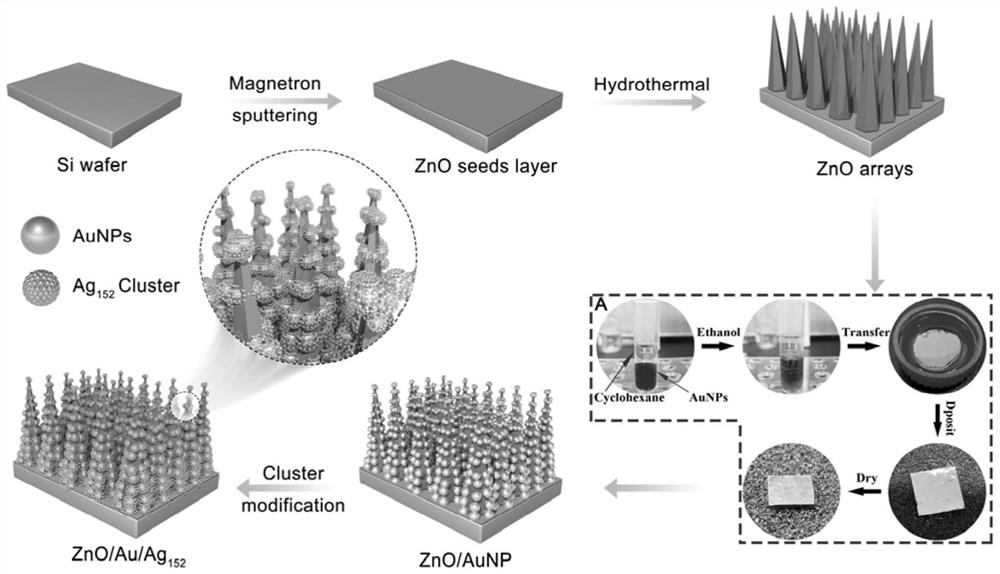
[0050] A protocol for the preparation of a novel reusable Raman-enhanced substrate.

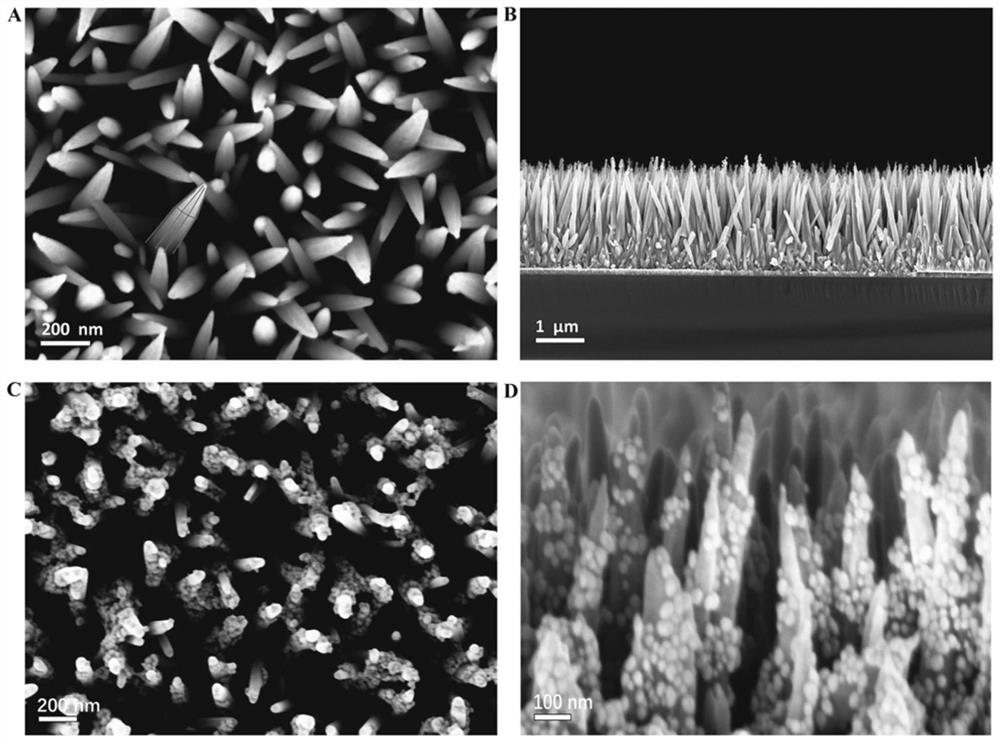
[0051] (1) ZnO seed crystal preparation: magnetron sputtering method, 1) with P(111) type single crystal silicon wafer as the substrate, P(111) type single crystal silicon wafer (1×1cm 2 ) Before sputtering, use acetone to ultrasonically clean for 15 minutes, rinse with deionized water, and anhydrous ethanol for 15 minutes, rinse with deionized water, and ultrasonically clean with deionized water for 15 minutes to ensure that the surface ions are completely removed. Blow dry and store in a vacuum. 2) Sputtering A ZnO ceramic target with a purity higher than 99.99% is used, and pre-sputtering is performed on it for 10 minutes to remove surface impurities. 3) Vacuum degree 3×10 -5 Torr, the vacuum atmosphere is Ar and O with a purity better than 99% 2 Gas mixture, the flow rate is 10:10 (sccm), the sputtering pressure is about 1Pa, the sputtering power is 100W, the deposition thickness is 10...

Embodiment 2

[0058] The SERS performance of the new three-dimensional substrate was evaluated by using crystal violet and rhodamine B molecules.

[0059] (1) Prepare 5×10 -4 M crystal violet aqueous solution, take 10 μL and drop it on ZnO array, ZnO / AuNPs substrate, ZnO / Au / Ag 152 The surface of the three-dimensional SERS substrate was dried for SERS detection (the Raman spectrometer was Derbyshire, and the excitation wavelength was 785nm). see test results Image 6 , by comparison, it can be found that the deposition of AuNPs has greatly improved the SERS signal intensity of the three-dimensional ZnO array. Subsequently, Ag 152 (SCH 2 CH 2 Ph) 60 With the deposition of nanoclusters, the intensity of SERS signal was further enhanced. It can be seen that the nanoclusters have greatly enhanced the SERS performance of the substrate.

[0060] (2) Prepare 5×10 -3 to 5×10 -12Rhodamine B aqueous solution of M for testing ZnO / AuNPs substrates and ZnO / Au / Ag 152 Detection limits for 3D SER...

Embodiment 3

[0067] The recyclability of the novel 3D substrate was evaluated using rhodamine 6G molecule.

[0068] (2) Prepare 1×10 -6 M of rhodamine 6G aqueous solution, take 2mL of the solution in a cuvette, use an ultraviolet absorbance photometer (UV-6300, MAPADA) to detect the absorbance, and record. Subsequently, under the assisted condition of ZnO / AuNPs substrate, the degradation reaction was carried out for 90min under the ultraviolet light (~254nm, 8w), and the absorbance of the solution was detected every ten minutes, and recorded. Such as Figure 9 As shown, with the prolongation of the ultraviolet radiation time, the absorbance of rhodamine 6G aqueous solution gradually decreases. At the same time, it can be seen in the inserted figure that the color of rhodamine 6G aqueous solution gradually becomes lighter, which also shows that rhodamine 6G molecules are assisted on the ZnO / AuNPs substrate. gradually degrades under these conditions.

[0069] (2) Using the same experiment...


PUM


Abstract

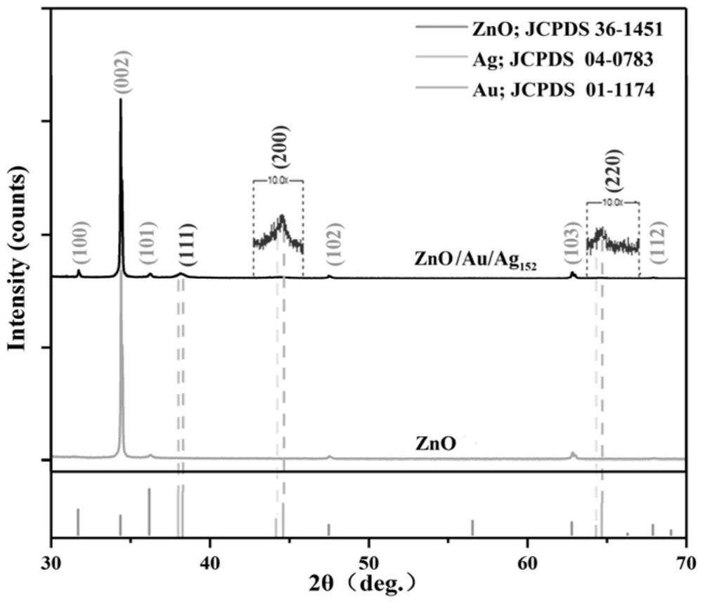
The invention discloses a reusable Raman enhanced substrate as well as a preparation method and application thereof. The method comprises the following steps: preparing ZnO crystal seeds; preparing aZnO array; preparing a ZnO / AuNPs substrate; and preparing the ZnO / Au / Ag152 three-dimensional SERS substrate. The grain size of the Ag152 (SCH2CH2Ph) 60 nanocluster is extremely small, so that hot spots on the original AuNPs film cannot be covered in the deposition process, and the hot spot density on the surface of the AuNPs film can be further increased; and the SERS performance of the original substrate is greatly improved. The substrate has good uniformity and signal reproducibility (RSD being equal to 6.95%), trace detection (5* 10<-12> M) of an analyte can be realized, an enhancement factor can reach 6.48*10 <9>, and recyclable detection can be realized. The method has the advantages of simple preparation process, low cost, high sensitivity, recyclability and the like, and is suitablefor mass production.

Description

technical field [0001] The invention belongs to the technical field of functionalized nanometer materials, and in particular relates to a reusable Raman enhanced substrate and its preparation method and application. Background technique [0002] Since surface-enhanced Raman scattering (SERS) can perform trace detection and provide unique fingerprint peaks for analytes, it has been widely used in various fields. SERS is mainly derived from the near field of surface plasmon polaritons generated by the interaction between the laser source and the SERS substrate. Therefore, the quality of the SERS substrate will directly affect the sensitivity and accuracy of detection. Usually, the construction of the substrate is a process of establishing SERS active sites (called "hot spots"). The "hot spots" mainly exist in the gaps between the metal nanoparticles and are accompanied by extremely high electric field enhancement. Therefore, the number of "hot spots" has a great influence o...

Claims


Application Information

Patent Timeline
IPC IPC(8): G01N21/65C01G9/02C01G9/03C23C14/35C23C14/08C23C14/58B22F9/24B22F1/00B82Y30/00B82Y40/00B82Y15/00
CPCG01N21/658C01G9/02C01G9/03C23C14/35C23C14/086C23C14/5806B22F9/24B82Y30/00B82Y40/00B82Y15/00B22F1/054
Inventor 胡勇军王俊杰余星星庄秀眉王琪胡婕妤
Owner SOUTH CHINA NORMAL UNIVERSITY
Learn More