Protective film frame, preparation method thereof and protective film assembly
A protective film and frame technology, which is applied in the photomechanical process of photomechanical processing of originals, patterned surface, ion implantation and plating, etc. It is suitable for large-scale production, the preparation method is simple, and the scattering rate is low.
- Summary
- Abstract
- Description
- Claims
- Application Information
AI Technical Summary
Problems solved by technology
Method used
Image
Examples
Embodiment 1
[0053] This embodiment provides a protective film frame, which includes a frame structure and a cladding layer covering the surface of the frame structure. Refer to attached figure 1 , the frame structure 110 of the protective film frame is used to support the protective film 120, and the cladding layer coated on the surface of the frame structure is formed of chromium or titanium dioxide.
[0054] The photomask plays a very important role in the photolithography process. It contains the chip pattern features of the entire substrate (silicon wafer), and performs 1:1 pattern replication during photolithography. figure 1 A photomask 100 and a masking layer 101 thereon are shown. In this embodiment, the photomask 100 is usually fused silica, and the masking layer 101 thereon is usually a chromium layer. The masking layer 101 forms the pattern formed on a substrate. Since the photomask 100 is the benchmark and blueprint for photolithographically reproduced patterns, any defect o...
Embodiment 2
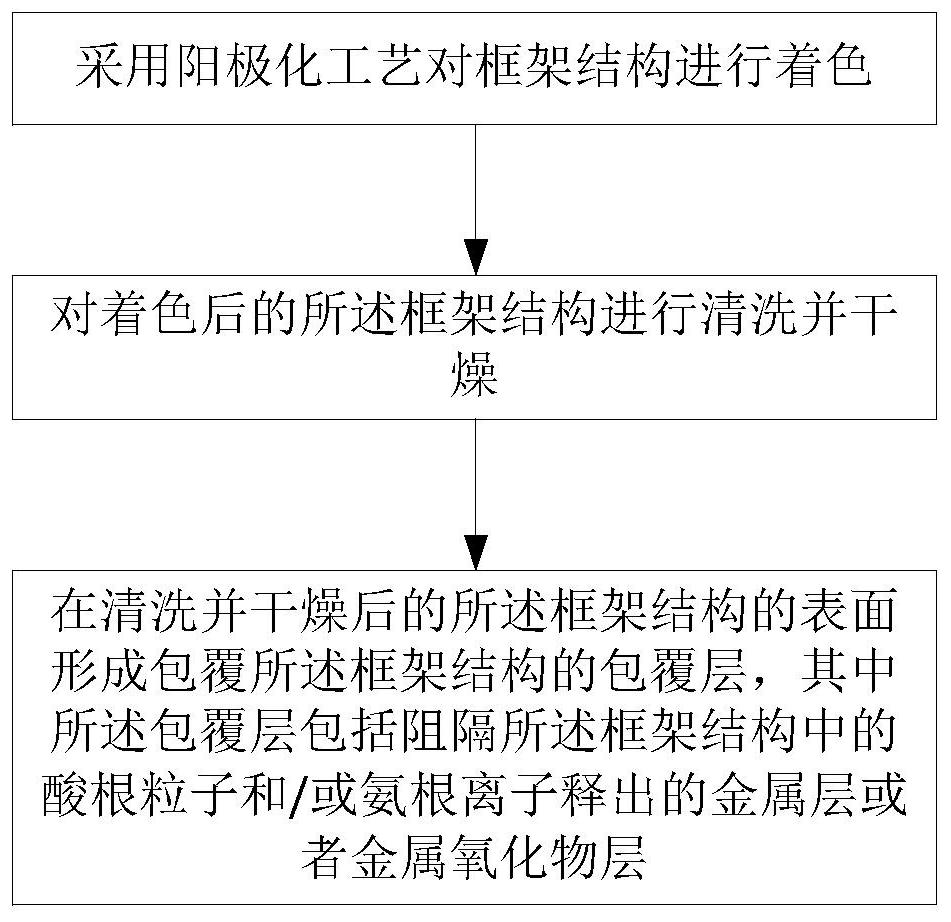
[0065] This embodiment provides a method for preparing a protective film frame, such as figure 2 As shown, the method includes the following steps:
[0066] Anodizing process is used to color the frame structure;
[0067] cleaning and drying the colored frame structure;
[0068] A cladding layer covering the framework structure is formed on the surface of the framework structure after cleaning and drying, wherein the cladding layer is formed of chromium or titanium dioxide.
[0069] In this embodiment, the frame structure is made by general processing technology, for example, according to the size required by the photolithography machine, more precisely, the aluminum alloy plate is cut according to the size of the photomask, and the frame structure is cut out. , and then perform mechanical polishing, alkali cleaning, pickling, and chemical polishing on the aluminum alloy frame structure. The chemically polished frame structure is anodized to refine it and color the frame s...
Embodiment 3
[0077] This embodiment provides a protective film assembly, also refer to the attached figure 1 , the protective film assembly includes a protective film frame and a protective film 120 . The protective film frame includes the protective film frame described in Embodiment 1, and the protective film frame also includes a frame structure 110 and a cladding layer coated on the surface of the frame structure, and the cladding layer is formed of chromium or titanium dioxide. The protective film 120 is adhered and supported on the frame structure 110 . For example, the protective film 120 can be adhered to the frame structure 110 by an adhesive and stretched tightly on the frame structure 110 .
[0078] Since the protective film assembly also includes the protective film frame described in Embodiment 1, during the exposure process, the acid radical / ammonium ion (SO 4 2- 、PO 4 3- and NH 4+ ) will not be released from the frame structure, thereby avoiding white haze (Haze) gener...
PUM
| Property | Measurement | Unit |
|---|---|---|
| thickness | aaaaa | aaaaa |
| thickness | aaaaa | aaaaa |
Abstract
Description
Claims
Application Information


