
Photoresist material for micro-nano processing as well as preparation and application thereof

A technology of photoresist and micro-nano structure, which is applied in the direction of photosensitive materials used for optomechanical equipment, technology for producing decorative surface effects, optomechanical equipment, etc., which can solve the incompatibility of photolithography technology and low resolution, etc. problem, to achieve the effect of widening the selection range, simple preparation method and various types

Pending Publication Date: 2021-06-11
HUAZHONG UNIV OF SCI & TECH
View PDF0 Cites 7 Cited by
  • Summary
  • Abstract
  • Description
  • Claims
  • Application Information

AI Technical Summary

Problems solved by technology

[0004] Aiming at the defects of the prior art, the purpose of the present invention is to provide a photoresist material for additive manufacturing of three-dimensional micro-nano structures of metal oxides, its preparation method and application, aiming to solve the problem of 3D metal oxide microstructures in the prior art. Technical issues such as light scattering, low resolution, and incompatibility with other lithography techniques due to the presence of high-mass fractions of metal oxide particles in the resin during the additive manufacturing of nanostructures

Method used


Image

  • Photoresist material for micro-nano processing as well as preparation and application thereof
  • Photoresist material for micro-nano processing as well as preparation and application thereof
  • Photoresist material for micro-nano processing as well as preparation and application thereof

Examples


preparation example Construction

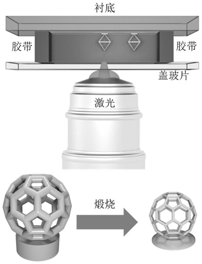
[0052] The present invention also provides the preparation method of described photoresist material, comprises the steps:

[0053] (1) Mix photosensitive resin monomer, organic acid and metal-organic framework material evenly to form solution A;

[0054] (2) Under the condition of avoiding light, add a photoinitiator into the solution A and stir evenly to obtain the photoresist material.

[0055] The good mutual solubility of metal organic framework materials and photosensitive resin monomers is very important for the preparation of three-dimensional metal oxide micro-nano structures by laser direct writing lithography. In the experiment of the present invention, it was found that the type of solvent was not suitable, or the dissolution time was not enough to cause the metal-organic framework When the material cannot be dissolved well, it cannot be formed by direct writing in subsequent laser direct writing, and an ideal three-dimensional structure cannot be obtained. If the ...

Embodiment 1

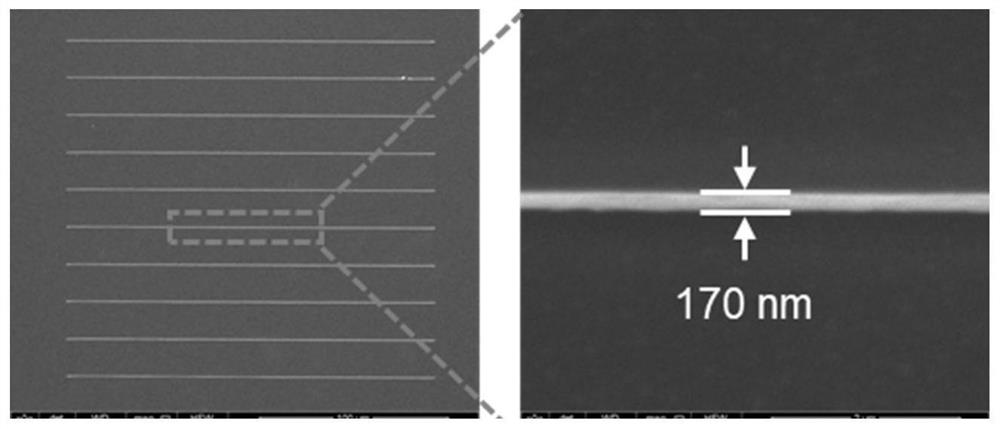
[0074] Dissolve 200 mg of ZIF-8 in 600 μL of acrylic acid and 500 μL of di(trimethylolpropane) tetraacrylic acid, and ultrasonicate in a water bath for 2 hours to obtain a uniform solution, then add 15 mg of photoinitiator benzil, photosensitizer 2-benzyl- 15 mg of 2-(dimethylamino)-4-morpholinobutaphenone was stirred with a magnetic stirrer for 30 min to obtain the photoresist, and the photoresist was dropped drop by drop on the quartz glass substrate with an interlayer. The developed femtosecond laser processing system additively manufactured a three-dimensional structure, then developed it in acrylic acid for five minutes, placed it in a diluent for five minutes, and dried it naturally to obtain a polymer with a three-dimensional micro-nano structure. The polymer with the three-dimensional micro-nano structure is placed in a small RTP annealing furnace, the heating rate is controlled at 5°C / min, under the oxygen flow, it is calcined at 550°C for 1 hour, and naturally cooled ...

Embodiment 2

[0078] Dissolve 50 mg of ZIF-67 in 600 μL of acrylic acid and 500 μL of bis(trimethylolpropane) tetraacrylic acid, and ultrasonicate for 2 hours in a water bath to obtain a uniform solution, then add 15 mg of photoinitiator benzil, photosensitizer 2-benzyl- 15 mg of 2-(dimethylamino)-4-morpholinobutaphenone was stirred with a magnetic stirrer for 30 min to obtain the photoresist, and the photoresist was dropped drop by drop on the quartz glass substrate with an interlayer. The developed femtosecond laser processing system additively manufactured a three-dimensional structure, then developed it in acrylic acid for five minutes, placed it in a diluent for five minutes, and dried it naturally to obtain a polymer with a three-dimensional micro-nano structure. The polymer with the three-dimensional micro-nano structure is placed in a small RTP annealing furnace, the heating rate is controlled at 5°C / min, under the oxygen flow, calcined at 600°C for 1 hour, and naturally cooled to ro...


PUM

PropertyMeasurementUnit
widthaaaaaaaaaa

Abstract

The invention belongs to the technical field of micro-nano processing, and more specifically relates to a photoresist material for micro-nano processing, and preparation and application thereof. The preparation method comprises the following steps: dissolving a metal-organic framework material in a photosensitive resin monomer through an organic acid, matching with a photoinitiator to form a photoresist material, carrying out additive manufacturing on a three-dimensional micro-nano structure by using an ultrafast laser direct writing system, performing developing and airing, and carrying out high-temperature calcination to obtain the metal oxide of the three-dimensional micro-nano structure. The additive manufacturing method of the metal oxide three-dimensional micro-nano structure has the advantages that the photoresist is simple and easy to prepare, the method is suitable for an ultrafast laser direct writing system, the resolution ratio is high, the forming effect is good, and any complex three-dimensional structure can be machined. The metal oxide with the three-dimensional micro-nano structure prepared by the method is expected to have important application in the fields of photonic crystals, structural colors, metamaterials, three-dimensional sensors, three-dimensional integrated circuits and the like.

Description

technical field [0001] The invention belongs to the technical field of micro-nano processing, and more specifically relates to a photoresist material used for additive manufacturing of three-dimensional micro-nano structures of metal oxides, its preparation and application. Background technique [0002] Metal oxides represent an important class of materials used in modern society. These materials exhibit unique properties, such as piezoelectricity, superconductivity, and semiconductivity, which allow them to play an important role in almost all types of micro-nanosystems device technologies. Most current device designs use metal oxides as thin-film stacks, since most use conventional planar lithography techniques to pattern these materials, which substantially limits the achievable geometries. Several advanced fabrication techniques have been developed to create 3D architectures with varying degrees of success. A top-down approach in which micro / nanostructures are grown fr...

Claims


Application Information

Patent Timeline
Patent Type & Authority Applications(China)
IPC IPC(8): G03F7/027G03F7/004C01G9/02C01G51/04B81C1/00
CPCG03F7/027G03F7/004C01G9/02C01G51/04B81C1/00436C01P2004/03C01P2002/72C01P2002/85Y02P10/25
Inventor 熊伟刘敬伟邓春三张文广喻克望焦玢璋刘耘呈邓磊敏
Owner HUAZHONG UNIV OF SCI & TECH
Learn More