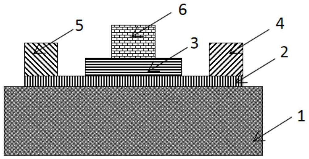
Junction field effect transistor based on tungsten disulfide/gallium antimonide and preparation method thereof
A field-effect transistor, junction technology, applied in transistors, semiconductor/solid-state device manufacturing, semiconductor devices, etc., can solve the problems of low defect state density, poor subthreshold swing, high dielectric constant, etc., to suppress interface defects The effect of producing, reducing impact, good stability
- Summary
- Abstract
- Description
- Claims
- Application Information
AI Technical Summary
Problems solved by technology
Method used
Image

Examples
Embodiment 1
[0038] WS-based 2 The preparation method of GaSb junction field effect transistor, concrete steps are as follows:
[0039] Step 1: Select a thermally oxidized silicon wafer as the substrate, first use ethanol, acetone, and deionized water to ultrasonicate for 5 minutes, then heat-treat the substrate on a heating platform at 300°C for 1 hour, and store it in a dry environment;
[0040] Step 2: Immerse the P-type GaSb nanowires grown on the glass substrate in anhydrous ethanol for 10-15s to disperse them, drop the dispersed liquid on the surface of the substrate, first spin-coat at 600rpm for 8 seconds, and then spin-coat at 2000rpm Coated for 50 seconds to obtain the desired P-type GaSb nanowires on the substrate surface.
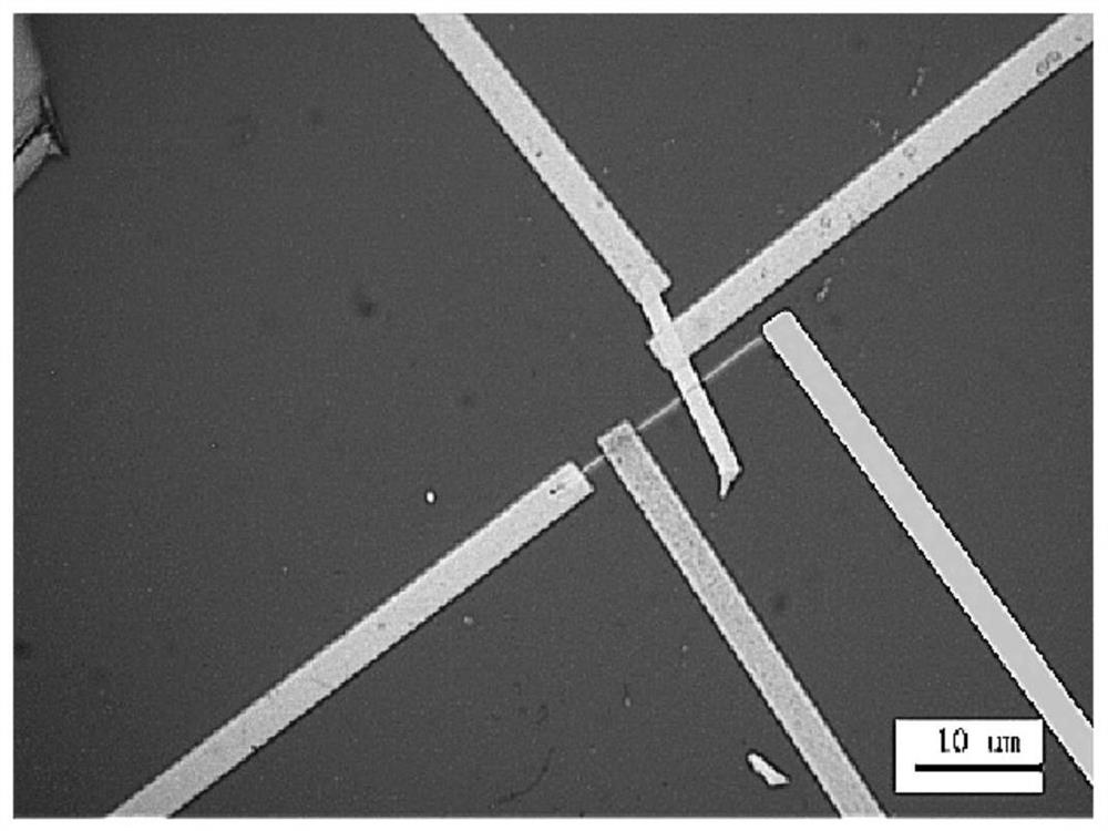
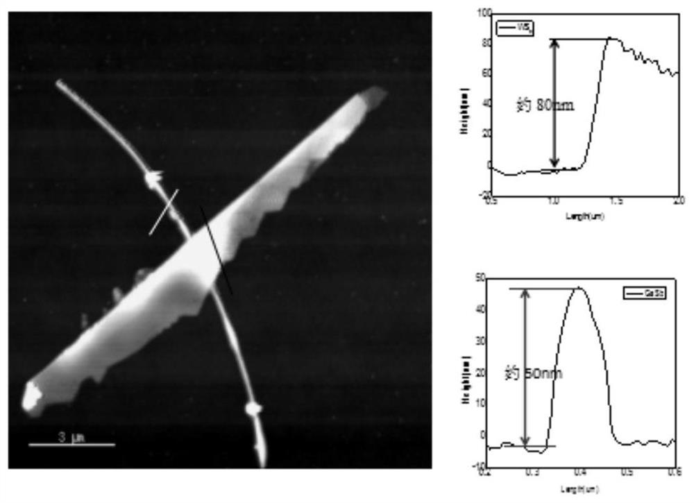
[0041] Step 3: Attach a smooth-surfaced PDMS membrane on the upper surface of the glass slide and prepare the N-type WS membrane obtained by mechanical exfoliation 2 Adhesive tape for thin film samples, stick the tape tightly on the PDMS membrane to make N...
PUM
| Property | Measurement | Unit |
|---|---|---|
| Thickness | aaaaa | aaaaa |
| Thickness | aaaaa | aaaaa |
| Thickness | aaaaa | aaaaa |
Abstract
Description
Claims
Application Information