

BJT based on two-dimensional transition metal chalcogenide and preparation method thereof
A technology of transition metal chalcogenides and compounds, which is applied in the manufacture of semiconductor/solid-state devices, semiconductor devices, electrical components, etc., can solve the problems of difficult precise control of doping concentration, device limitations, and film damage, and achieve simple structure and reduced damage degree, the effect of improving device performance
- Summary
- Abstract
- Description
- Claims
- Application Information
AI Technical Summary
Problems solved by technology
Method used
Image

Examples
preparation example Construction
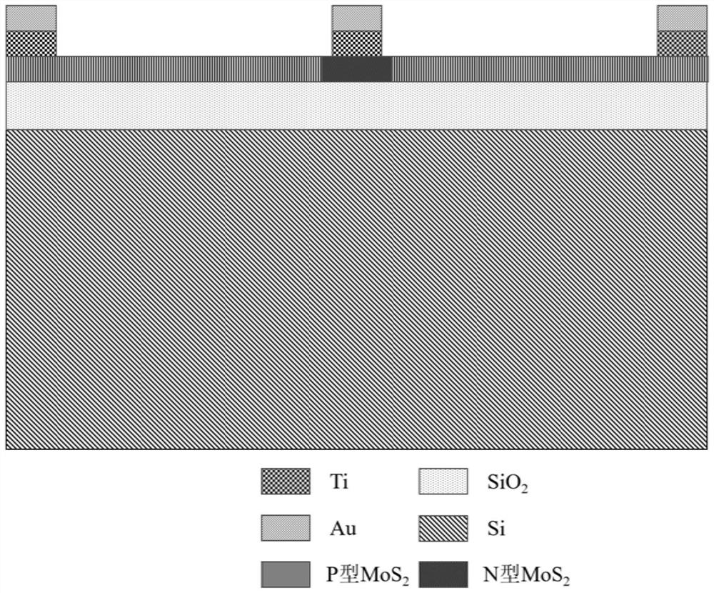
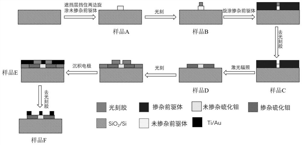
[0065] The present invention also provides the preparation method of the above-mentioned BJT based on two-dimensional transition metal chalcogenides, such as image 3 shown, including the following steps:
[0066] (S1) Prepare a shielding layer on the upper surface of the dielectric layer in the single crystal silicon substrate with the dielectric layer, exposing only the middle region of the dielectric layer;
[0067] In some optional embodiments, two pieces of adhesive tape can be pasted directly on both sides of the medium layer as a shielding layer, exposing the strip-shaped area in the middle;
[0068] (S2) Spin-coat the first precursor solution on the dielectric layer prepared with the shielding layer, dry after soaking, and obtain sample A;
[0069] The first precursor solution contains sulfur and two-dimensional transition metal elements;
[0070] (S3) After spin-coating photoresist on the upper surface of sample A, remove the shielding layer to obtain sample B;
[...
Embodiment 1
[0092] Dissolve 200mg of thiourea and 80mg of molybdenum pentachloride in 3.75mL of isopropanol, the magnetic stirring speed is 1500rpm, the stirring time is 1h, and the dissolution temperature is 70°C to obtain the precursor solution A. Use acetone to ultrasonically clean the 300 μm thick p-type silicon with a 100nm-thick silicon dioxide dielectric layer on the upper surface to remove organic dirt on the substrate and dielectric layer, then use alcohol to clean the substrate to remove the acetone on the surface, and finally use deionization Rinse with water and blow dry with nitrogen gun. Paste two pieces of adhesive tape on the surface of the substrate as a masking layer, exposing the strip-shaped area. Take 0.1 mL of precursor solution A, spin-coat on the upper surface of the substrate dielectric layer, soak for 60 s, and then spin-coat at 3000 rpm for 30 s. Then dry at 90°C for 1 min. Then, AZ5214 photoresist was spin-coated on the surface of the sample, and a suitable m...
Embodiment 2
[0094] Dissolve 200mg of thiourea and 50mg of molybdenum pentachloride in 3.75mL of isopropanol, the magnetic stirring speed is 1500rpm, the stirring time is 1h, and the dissolution temperature is 70°C to obtain the precursor solution A. Use acetone to ultrasonically clean the 300 μm thick p-type silicon with a 100nm-thick silicon dioxide dielectric layer on the upper surface to remove organic dirt on the substrate and dielectric layer, then use alcohol to clean the substrate to remove the acetone on the surface, and finally use deionization Rinse with water and blow dry with nitrogen gun. Paste two pieces of adhesive tape on the surface of the substrate as a masking layer, exposing the strip-shaped area. Take 0.1 mL of precursor solution A, spin-coat on the upper surface of the base dielectric layer, soak for 30 s, and then spin-coat at 1500 rpm for 60 s. Then dry at 90°C for 2min. Then, AZ5214 photoresist was spin-coated on the surface of the sample, and a suitable mask wa...
PUM
| Property | Measurement | Unit |
|---|---|---|
| Thickness | aaaaa | aaaaa |
| Thickness | aaaaa | aaaaa |
| Thickness | aaaaa | aaaaa |
Abstract
Description
Claims
Application Information