A two-dimensional semiconductor conjugated polymer material and its preparation and application in ultrafast laser protection

A conjugated polymer and two-dimensional semiconductor technology, applied in the field of two-dimensional materials, can solve the problems of hindering electron transport, π-π stacking hindering electron transport, poor response, etc., and achieve excellent broadband absorption, good optical properties, and high thermal stability Effects on sexuality and environmental stability

Active Publication Date: 2022-05-17
TONGJI UNIV
View PDF0 Cites 0 Cited by
  • Summary
  • Abstract
  • Description
  • Claims
  • Application Information

AI Technical Summary

Problems solved by technology

In the application of ultrafast optics of two-dimensional materials, it is easy to hinder the transmission of electrons due to π-π stacking, resulting in relatively poor response under ultrafast pulse width lasers
Although there have been researches on the synthesis of semiconductor conjugated polymer materials, most of them exist in bulk form, which cannot solve the problem that their π-π stacking hinders the transport of electrons.

Method used


Image

  • A two-dimensional semiconductor conjugated polymer material and its preparation and application in ultrafast laser protection
  • A two-dimensional semiconductor conjugated polymer material and its preparation and application in ultrafast laser protection
  • A two-dimensional semiconductor conjugated polymer material and its preparation and application in ultrafast laser protection

Examples


Embodiment 1

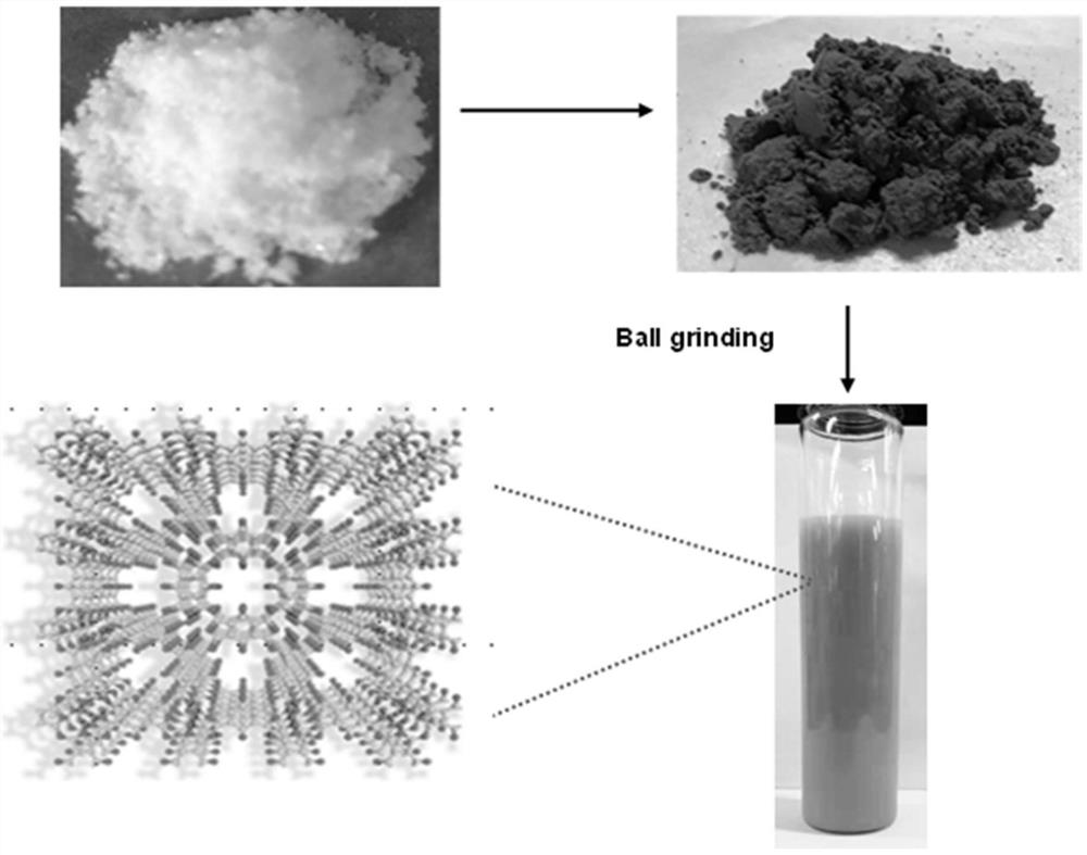
[0035] A method for preparing a two-dimensional semiconductor conjugated polymer material, specifically comprising the following steps:

[0036] (1) Take 10 g of urea, 2.5 g of ammonium chloride, 3 g of pyromellitic dianhydride, 0.5 g of ammonium molybdate, and 1.5 g of phthalic anhydride, grind for about 20 minutes, and mix well to obtain a raw material mixture;

[0037] (2) Add the above-mentioned raw material mixture into the crucible, and then place it in a muffle furnace, and the muffle furnace raises the temperature from room temperature to about 350°C at a rate of 10°C / min, and calcines for 2.5 hours to obtain a crude product;

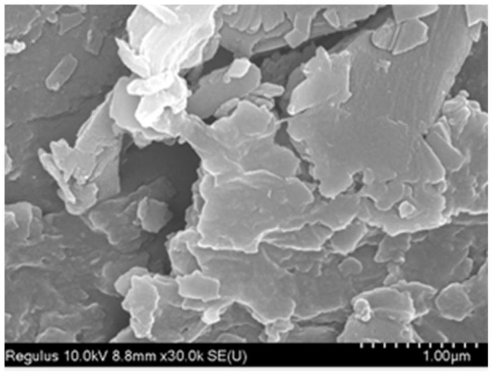
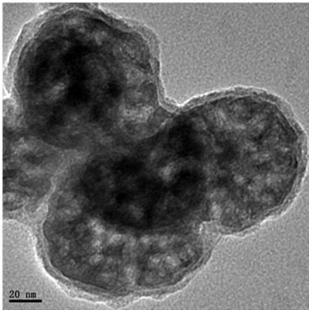
[0038] (3) Wash and filter the crude product repeatedly with methanol and distilled water until the filtrate is colorless, then disperse the filtered solid phase product in distilled water, place the resulting dispersion in a grinding bowl made of zirconia, add The zirconium pellets were ball milled for 4 hours at a rotational speed of 2500 rpm,...

Embodiment 2

[0042] A method for preparing a two-dimensional semiconductor conjugated polymer material, specifically comprising the following steps:

[0043] (1) Take 10 g of urea, 2.5 g of ammonium chloride, 6 g of pyromellitic dianhydride, 0.5 g of ammonium molybdate, and 1.5 g of phthalic anhydride, grind for about 20 minutes, and mix well to obtain a raw material mixture;

[0044] (2) The crucible is placed in a muffle furnace, and the temperature of the muffle furnace is raised from room temperature to about 350° C. at a rate of 10° C. / min, and calcined for 2.5 hours to obtain a crude product.

[0045] (3) The crude product was repeatedly washed and filtered with methanol until the filtrate was colorless, and then filtered to obtain a powder product.

[0046] (4) Disperse the powder product in ethanol, place the dispersion in a grinding bowl made of zirconia, add zirconia balls, and ball mill for 4 hours at a speed of 2500.

[0047] Take the two-dimensional semiconductor conjugated pol...

Embodiment 3

[0050] A method for preparing a two-dimensional semiconductor conjugated polymer material and its ultrafast laser test, specifically including the following steps:

[0051] (1) Take 10g of urea, 2.5g of ammonium chloride, 6g of pyromellitic dianhydride, 0.5g of ammonium molybdate, and 1.5g of phthalic anhydride, grind for about 20min, and mix well to obtain the raw material mixture and add it to the crucible;

[0052] (2) The crucible is placed in a muffle furnace, and the temperature of the muffle furnace is raised from room temperature to about 350° C. at a rate of 10° C. / min, and calcined for 2.5 hours to obtain a crude product.

[0053] (3) The crude product is washed and filtered repeatedly in an organic solvent until the filtrate is colorless. The organic solvent is dichloromethane and dimethyl sulfoxide, and a filtered powder product is obtained.

[0054] (4) Disperse the filtered powder product in ethanol, place the dispersion in a grinding bowl made of zirconia, add z...


PUM

PropertyMeasurementUnit
thicknessaaaaaaaaaa
specific surface areaaaaaaaaaaa

Abstract

The invention relates to a two-dimensional semiconductor conjugated polymer material and its preparation and application in ultrafast laser protection. The preparation process is specifically: using a solid-phase polymerization reaction assisted by an end-capping agent, using small organic molecules as monomers , under the action of a catalyst, it undergoes high-temperature calcination and polymerization in the air environment, and after the polymerization is completed, a two-dimensional semiconductor conjugated polymer material is obtained by mechanical exfoliation. Compared with the prior art, the material of the present invention has an ultra-thin two-dimensional sheet structure, good crystallinity, a super-large conjugate plane, and can rapidly delocalize electrons. The region exhibits nonlinear absorption characteristics, specifically manifested as anti-saturation absorption behavior; at the same time, it is easy to operate, easy to control the reaction conditions, and easy to produce on a large scale.

Description

technical field [0001] The invention belongs to the technical field of two-dimensional materials, and relates to a two-dimensional semiconductor conjugated polymer material and its preparation and application in ultrafast laser protection. Background technique [0002] Since T.Maiman first discovered the ruby ​​laser in 1960, ultrafast laser, as an important branch of optics, has been widely used in communications, military, medicine, protection and industry. Ultrafast laser sensitive materials, especially ultrafast laser protective materials aroused great concern of scientists. However, traditional optically sensitive materials are difficult to meet the growing application requirements. In order to solve this problem, two-dimensional materials, due to their excellent optical properties such as ultrafast broadband optical response, obvious optical polarization degree, and strong excitonic effect in ultra The field of fast optics has been greatly developed. Due to the insta...

Claims


Application Information

Patent Timeline
Patent Type & Authority Patents(China)
IPC IPC(8): C08G73/10G02F1/361
CPCC08G73/1007C08G73/1082G02F1/3611Y02E10/549
Inventor 张弛刘芳伏露露
Owner TONGJI UNIV
Why Eureka
Try Eureka