Method for rapidly removing sediments on back surface of wafer in epitaxial process of silicon carbide

An epitaxial wafer, silicon carbide single crystal technology, applied in chemical instruments and methods, single crystal growth, crystal growth and other directions, can solve the problems affecting the production efficiency of silicon carbide epitaxial wafers, increase manufacturing costs, etc., and achieve cost control and improvement. Production efficiency, effect of reduction in removal process time

Active Publication Date: 2021-12-17
DONGGUAN TIANYU SEMICON TECH
View PDF7 Cites 2 Cited by
  • Summary
  • Abstract
  • Description
  • Claims
  • Application Information

AI Technical Summary

Problems solved by technology

The above-mentioned white spot problem caused by reactive deposition on the back of the wafer seriousl...

Method used


Image

  • Method for rapidly removing sediments on back surface of wafer in epitaxial process of silicon carbide

Examples


Embodiment 1

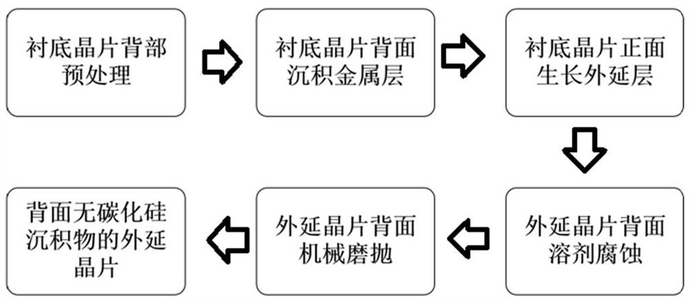
[0025] Embodiment one: if figure 1 Shown, a kind of method that removes the wafer back side deposition in the silicon carbide epitaxy process fast, comprises the following steps:

[0026] S1) Pretreatment of the substrate wafer: the back side (non-epitaxial growth surface) of the silicon carbide single crystal substrate wafer is cleaned, hydrogen etched and / or polished; this step is aimed at cleaning the stains on the back side of the substrate wafer and improve surface flatness; if the incoming quality of the substrate wafer meets the requirements of actual use, the polishing and hydrogen etching processes can be omitted.

[0027] The cleaning of this solution is to use automatic tank cleaning equipment to clean the silicon carbide substrate wafer. The automatic tank cleaning equipment can clean both sides of the substrate wafer at the same time. The cleaning steps are acetone ultrasonic immersion cleaning, sulfuric acid and Hydrogen peroxide mixed solution heating soaking, ...

Embodiment 2

[0035] Embodiment two: if figure 1 Shown, a kind of method that removes the wafer back side deposition in the silicon carbide epitaxy process fast, comprises the following steps:

[0036] S1) Pretreatment of the substrate wafer: cleaning the back of the silicon carbide single crystal substrate wafer; this step aims to clean the stains on the back of the substrate wafer and improve the surface flatness;

[0037] Cleaning is to use automatic tank cleaning equipment to clean the silicon carbide substrate wafer. The automatic tank cleaning equipment can clean both sides of the substrate wafer at the same time. The cleaning steps are acetone ultrasonic immersion cleaning, sulfuric acid and hydrogen peroxide mixed solution Heating soaking, ammonia water and hydrogen peroxide mixed solution heating soaking, deionized water ultrasonic cleaning. The processing time of each step was 20 min, 10 min, 10 min and 20 min in turn.

[0038] S2) Formation of the metal layer: the magnetron spu...

Embodiment 3

[0041] Embodiment three: as figure 1 Shown, a kind of method that removes the wafer back side deposition in the silicon carbide epitaxy process fast, comprises the following steps:

[0042] S1) Substrate wafer pretreatment; the back of the silicon carbide single crystal substrate wafer is cleaned, hydrogen etched and pre-polished; this step aims to clean the stains on the back of the substrate wafer and improve the surface flatness; if the substrate The quality of incoming wafers meets the requirements of actual use, and the polishing and hydrogen etching processes can be omitted.

[0043] Cleaning is to use automatic tank cleaning equipment to clean the silicon carbide substrate wafer. The automatic tank cleaning equipment can clean both sides of the substrate wafer at the same time. The cleaning steps are acetone ultrasonic immersion cleaning, sulfuric acid and hydrogen peroxide mixed solution Heating soaking, ammonia water and hydrogen peroxide mixed solution heating soaki...


PUM


Abstract

The invention discloses a method for rapidly removing sediments on the back surface of a wafer in an epitaxy process of a silicon carbide . The method comprises the following steps: S1) pretreating a substrate wafer: carrying out cleaning, hydrogen etching and/or polishing pretreatment on the back surface (non-epitaxial growth surface) of a silicon carbide single crystal substrate wafer; S2) forming a metal layer: depositing a metal or alloy on the back surface of the silicon carbide single crystal substrate wafer by adopting a magnetron sputtering method to form the metal layer; S3) forming a silicon carbide epitaxial wafer: growing a silicon carbide epitaxial layer on the epitaxial growth surface of the silicon carbide single crystal substrate wafer through a chemical vapor deposition method to obtain the silicon carbide epitaxial wafer; and S4) removing the metal layer: removing the metal layer on the back surface of the silicon carbide epitaxial wafer and the sediments attached to the surface of the metal layer in a solvent corrosion manner. According to the invention, after the method is adopted, the time of the process for removing the sediments on the back surface of the wafer is greatly shortened, the production efficiency can be effectively improved, and the cost control of the silicon carbide epitaxial wafer is facilitated.

Description

technical field [0001] The invention relates to the technical field of crystal synthesis, in particular to a method for quickly removing deposits on the back of a wafer during the silicon carbide epitaxy process. Background technique [0002] Silicon carbide single crystal material has the advantages of high thermal conductivity, high breakdown field strength, high saturation electron drift rate and high bonding energy, etc., which can well meet the needs of modern electronic technology for high temperature, high power, high voltage, high frequency and high radiation. applications requiring harsh conditions. Unlike traditional silicon material devices, silicon carbide devices cannot be directly fabricated on silicon carbide single crystal materials. High-quality epitaxial layers must be grown on single crystal substrates, and then devices of various structures are fabricated on the epitaxial layers. [0003] Among various silicon carbide epitaxial layer preparation methods,...

Claims


Application Information

Patent Timeline
IPC IPC(8): C30B29/36C30B25/18H01L21/02
CPCC30B29/36C30B25/186H01L21/02008H01L21/02016H01L21/02019
Inventor 丁雄傑韩景瑞李锡光张锐军
Owner DONGGUAN TIANYU SEMICON TECH
Why Eureka
Try Eureka