Method for preparing large-area high-performance n-type two-dimensional molybdenum telluride field effect transistor array

A transistor array and molybdenum telluride field technology, which is applied in the field of preparing large-area high-performance n-type two-dimensional molybdenum telluride field effect transistor arrays, can solve problems such as unsatisfactory doping effects, achieve low contact resistance, and improve injection efficiency , the effect of improving performance

Pending Publication Date: 2022-03-11
PEKING UNIV
View PDF0 Cites 2 Cited by
  • Summary
  • Abstract
  • Description
  • Claims
  • Application Information

AI Technical Summary

Problems solved by technology

The methods of n-type doping molybdenum telluride reported in the existing literature mainly include chemical doping, atomic layer deposition of aluminum oxide, etc., but these literature reports are usually limited to the preparation of a single device, and the doping effect is not ideal.

Method used


Image

  • Method for preparing large-area high-performance n-type two-dimensional molybdenum telluride field effect transistor array
  • Method for preparing large-area high-performance n-type two-dimensional molybdenum telluride field effect transistor array
  • Method for preparing large-area high-performance n-type two-dimensional molybdenum telluride field effect transistor array

Examples


Embodiment Construction

[0027] The present invention will be further elaborated below through specific implementation examples in conjunction with the accompanying drawings.

[0028] In this embodiment, the method for preparing a large-area high-performance n-type two-dimensional molybdenum telluride field-effect transistor array includes the following steps:

[0029] 1) Prepare silicon / silicon oxide substrate, SiO 2 The thickness is 285nm.

[0030] 2) A molybdenum thin film with a thickness of about 2 nm is deposited on the substrate by magnetron sputtering.

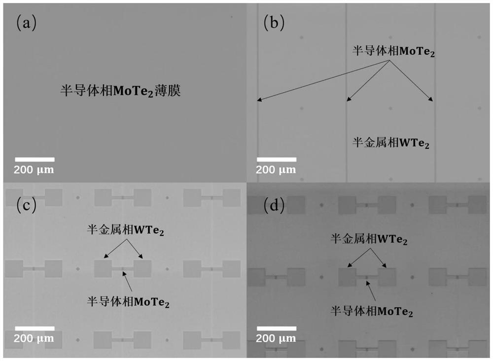
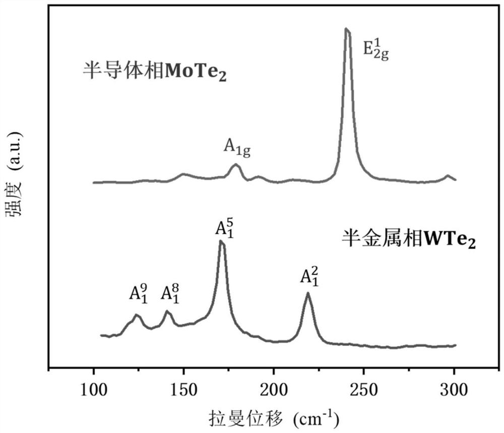
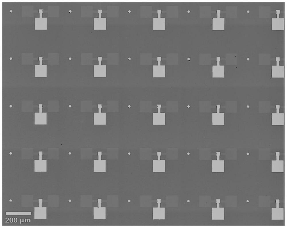
[0031] 3) Carry out chemical vapor deposition to the sample: put appropriate amount of tellurium powder and the sample in the quartz boat, then put the quartz boat into the tube furnace, so that the tellurium powder flows up the sample; keep the airflow of 7 sccm hydrogen and 5 sccm argon, heat tube furnace to raise the temperature to 630°C after 20 minutes, keep the chamber at a constant temperature for 3 hours, and then cool down to room t...


PUM

PropertyMeasurementUnit
thicknessaaaaaaaaaa

Abstract

The invention discloses a method for preparing a large-area high-performance n-type two-dimensional molybdenum telluride field effect transistor array. The method comprises the following steps: growing a semiconductor phase molybdenum telluride thin film on a substrate, patterning the semiconductor phase molybdenum telluride thin film and growing a tungsten thin film to obtain a thin film in which metal tungsten and semiconductor phase molybdenum telluride are alternated, and changing the tungsten thin film into a semimetal phase tungsten telluride thin film through a chemical vapor deposition method; patterning again to obtain a discrete device array which takes semiconductor phase molybdenum telluride as a channel and semi-metal phase tungsten telluride as an electrode; and finally, performing n-type doping on the device through atomic layer deposition of a hafnium oxide thin film, and preparing a patterned top gate metal electrode to obtain a large-area high-performance n-type two-dimensional molybdenum telluride field effect transistor array. According to the method, the n-type doping effect on the two-dimensional molybdenum telluride is ideal, the doping degree is adjustable, meanwhile, the contact resistance of the source electrode and the drain electrode of the prepared device is low, the performance of the device is improved, and a foundation is provided for application of two-dimensional semiconductor materials in the field of integrated circuits and the like.

Description

technical field [0001] The invention relates to n-type doping of two-dimensional materials, preparation of low contact resistance source and drain electrodes and preparation of large-area field-effect transistor devices, in particular to a method for preparing a large-area high-performance n-type two-dimensional molybdenum telluride field-effect transistor array method and application. Background technique [0002] With the development of integrated circuits, the size of traditional silicon-based transistors is getting smaller and smaller, approaching its quantum limit and thermodynamic limit, and new materials are needed to continue Moore's Law. Since the thickness of two-dimensional semiconductor materials is reduced to only one or a few atomic layer thickness scales, the characteristic channel length where the short channel effect occurs can be further reduced. As a common two-dimensional material, molybdenum telluride material exhibits p-type in air and is easy to be pr...

Claims


Application Information

Patent Timeline
Patent Type & Authority Applications(China)
IPC IPC(8): H01L21/34H01L21/02C23C14/04C23C14/18C23C14/30C23C14/35C23C16/04C23C16/30C23C16/40C23C16/455C23C28/00
CPCH01L29/66969H01L21/02562H01L21/0262H01L21/02664C23C14/35C23C14/042C23C14/185C23C16/305C23C16/042C23C16/405C23C16/45525C23C14/30C23C28/40C23C28/322C23C28/345
Inventor 戴伦程智轩贾雄辉
Owner PEKING UNIV
Why Eureka
Try Eureka