Preparation method of PDMS in-situ wrinkled antireflection film and monochromatic light organic light emitting diode
A technology of light-emitting diodes and anti-reflection coatings, which is applied in the manufacture of semiconductor/solid-state devices, electrical components, and electrical solid-state devices. Light extraction efficiency and final external quantum efficiency, the effects of a wide range of options
- Summary
- Abstract
- Description
- Claims
- Application Information
AI Technical Summary
Problems solved by technology
Method used
Image
Examples
Embodiment 1
[0055] In this example,
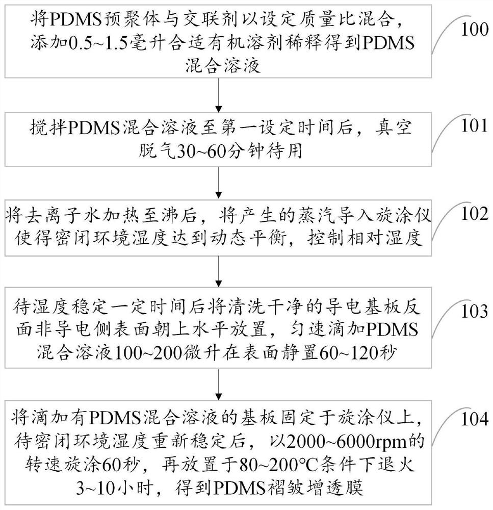
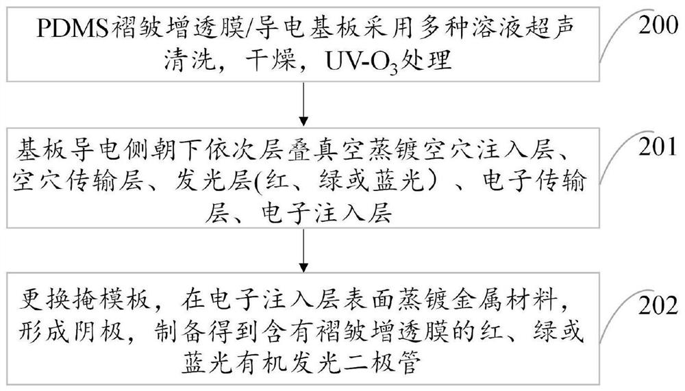
[0056] see figure 1 and figure 2 , a method for preparing a PDMS in-situ wrinkled anti-reflection film and a monochromatic organic light-emitting diode, comprising the steps of:
[0057] Step 100: According to the ratio of the mass ratio of PDMS prepolymer and PDMS crosslinking agent to 10:1, weigh 3.3 g of PDMS prepolymer and PDMS crosslinking agent, add them into clean transparent reagent bottles, and take 0.5 g respectively mL, 1.0mL and 1.5mL of chloroform were mixed with PDMS solution;
[0058] Step 101: Stir evenly, seal, and place the mixed solution in a moderate vacuum environment for degassing for 1 hour;
[0059] Step 102: After heating the deionized water to boiling, the generated steam is introduced into the spin coater so that the humidity in the airtight environment reaches a dynamic balance, and the relative humidity is controlled to be 75%;
[0060] Step 103: After ultrasonically cleaning the ITO glass substrate with detergent, ac...
Embodiment 2
[0069] This embodiment is basically the same as Embodiment 1, especially in that:
[0070] In this embodiment, a method for preparing a PDMS in-situ wrinkled anti-reflection film and a monochromatic organic light-emitting diode includes the following steps:
[0071] Step 100: According to the ratio of the mass ratio of PDMS prepolymer and PDMS crosslinking agent to 10:1, weigh 3.3g of PDMS prepolymer and PDMS crosslinking agent, add it to a clean transparent reagent bottle, and take 1.0mL Chloroform is mixed with PDMS solution;
[0072] Step 101~step 200: this step is the same as that of Embodiment 1;
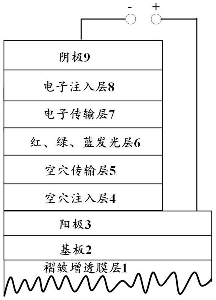
[0073] Step 201: Place the conductive side of the substrate in step 200 down in a vacuum evaporation chamber to sequentially evaporate various functional layers, including MoO 3 (5nm) / NPB(35nm) / mCP(5nm) / DMAC-DPS:DPEPO(10wt%, 20nm) / DPEPO(10nm) / Bphen(40nm) / LiF(0.8nm);
[0074] Step 202: Finally, replace the mask to vapor-deposit cathode metal Al to prepare an electrode cathode...
PUM
| Property | Measurement | Unit |
|---|---|---|
| thickness | aaaaa | aaaaa |
| thickness | aaaaa | aaaaa |
| thickness | aaaaa | aaaaa |
Abstract
Description
Claims
Application Information


