Heterojunction solar cell and preparation method thereof

A solar cell and heterojunction technology, applied in the field of solar cells, can solve the problems affecting the photoelectric conversion efficiency of heterojunction solar cells, the transparent conductive oxide film is easily damaged, and the battery contact resistance/series resistance is large, so as to achieve improvement Photoelectric conversion efficiency, avoiding poor adhesion, and reducing production costs

Pending Publication Date: 2022-05-06
SUZHOU MAXWELL TECH CO LTD
View PDF1 Cites 0 Cited by
  • Summary
  • Abstract
  • Description
  • Claims
  • Application Information

AI Technical Summary

Problems solved by technology

[0003] However, in the existing preparation technology, the obtained heterojunction solar cells tend to form high-resistance interfaces, which leads to a large contact resistance / series resistance of the cells; or the prepared metal grid wire electrodes are easy to fall off
In addition, in the preparation process of the existing heterojunction solar cells, the transparent conductive oxide film is easily damaged when the metal electrode is prepared by the electroplating process, especially the transparent conductive oxide film with a lower price is more likely to be completely destroyed , affecting the photoelectric conversion efficiency of heterojunction solar cells

Method used


Image

  • Heterojunction solar cell and preparation method thereof
  • Heterojunction solar cell and preparation method thereof
  • Heterojunction solar cell and preparation method thereof

Examples


preparation example Construction

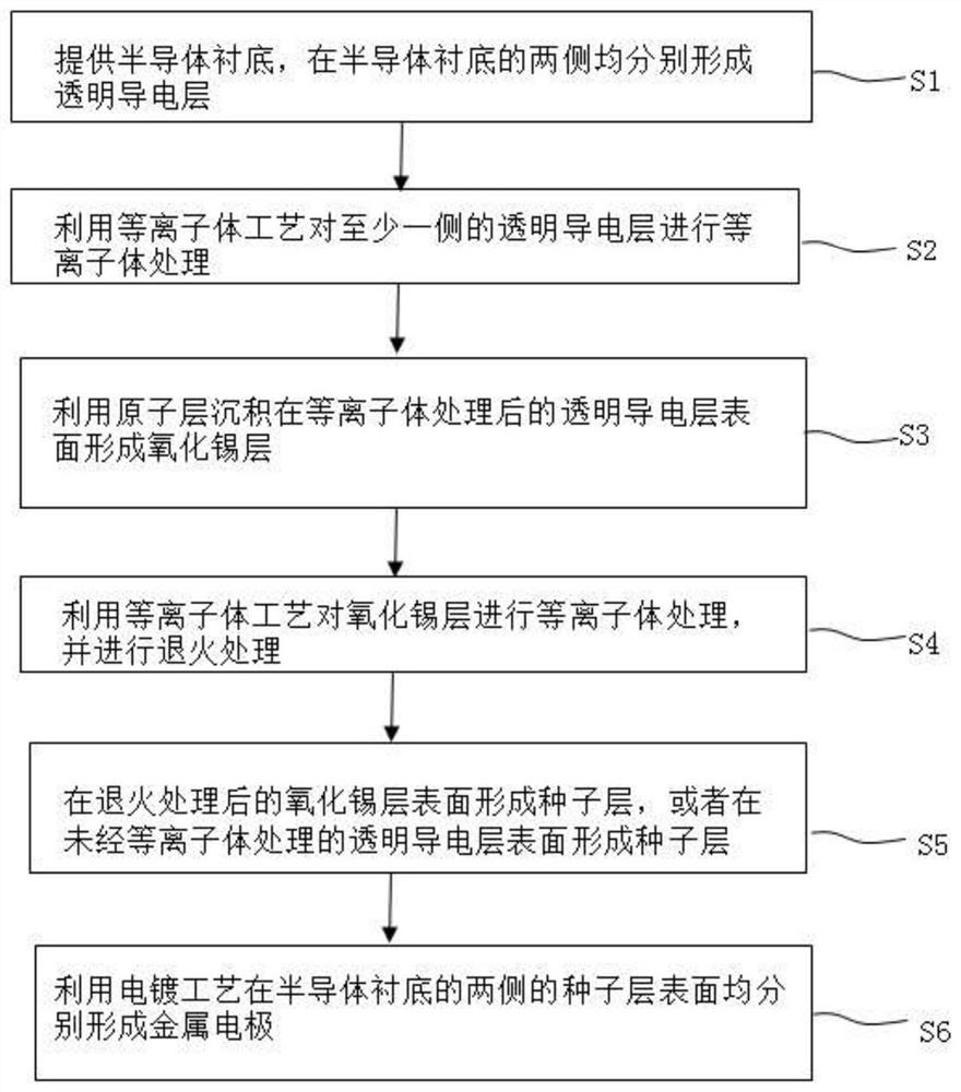
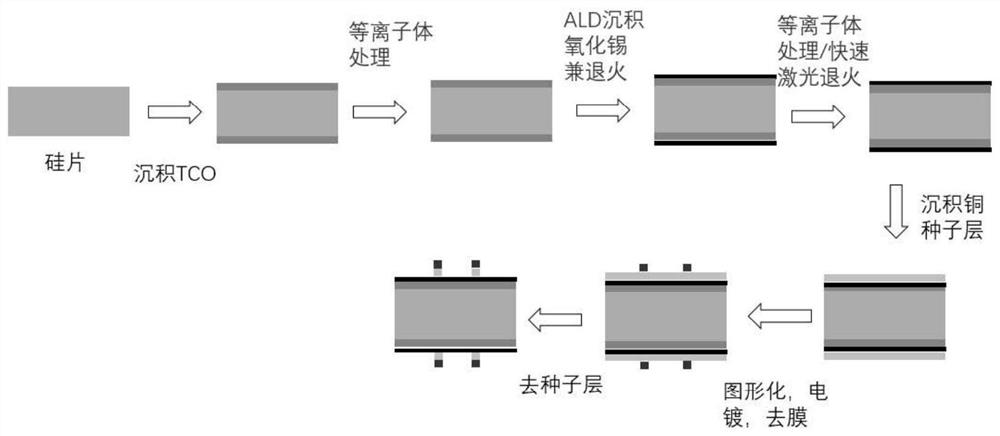
[0040] see figure 1 or figure 2 As shown, in some embodiments, a method for preparing a heterojunction solar cell is provided, the method comprising:

[0041] S1. Provide a semiconductor substrate, and form transparent conductive layers on both sides of the semiconductor substrate;

[0042] S2. Using a plasma process to perform plasma treatment on at least one side of the transparent conductive layer;

[0043] S3, forming a tin oxide layer on the surface of the plasma-treated transparent conductive layer by atomic layer deposition;

[0044] S4, using a plasma process to perform plasma treatment on the tin oxide layer, and perform annealing treatment;

[0045] S5, forming a seed layer on the surface of the annealed tin oxide layer, or forming a seed layer on the surface of the non-plasma-treated transparent conductive layer;

[0046] S6 , forming metal electrodes on the surfaces of the seed layers on both sides of the semiconductor substrate by using an electroplating proc...

Embodiment 1

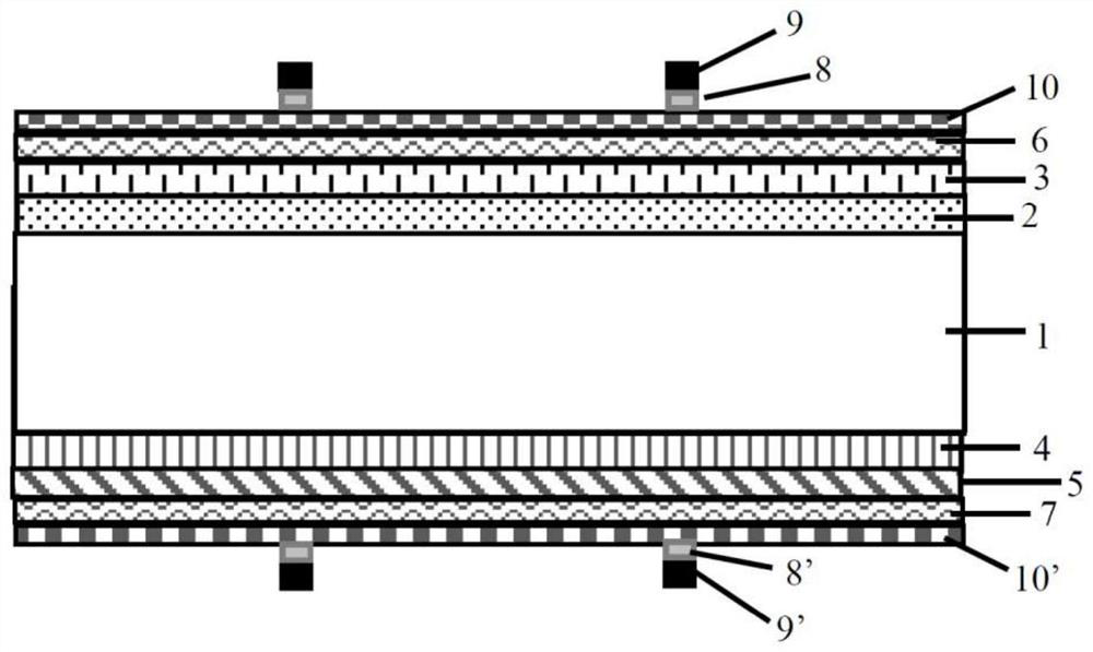
[0090] S11. Depositing the first intrinsic amorphous silicon layer 2 and the first doped layer 3 (such as phosphorous-doped amorphous or microcrystalline silicon layer), and deposit a second intrinsic amorphous silicon layer 4 and a second doped layer 5 (such as a boron-doped amorphous or microcrystalline silicon layer) in sequence on the back of the semiconductor substrate 1 .

[0091] Wherein, the deposition conditions of the first intrinsic amorphous silicon layer or the second intrinsic amorphous silicon layer are: the power supply is 500W, the gas flow ratio of hydrogen to silane (hydrogen dilution ratio) is 9.5:1, and the pressure is 50Pa. The substrate temperature was 220°C. The deposition conditions of the phosphorus-doped amorphous or microcrystalline silicon layer are: the power supply is 400W, the gas flow ratio of hydrogen to silane (hydrogen dilution ratio) is 5.5:1, and the gas flow ratio of phosphine to silane (phosphorus to silicon ratio) The ratio is 1:109, t...

Embodiment 2

[0101] The preparation method of embodiment 2 is basically the same as that of embodiment 1, and the similarities are not repeated, and the difference is:

[0102] In Example 2, in step S12, a magnetron sputtering coating device is used to deposit a TCO film, and argon and oxygen are introduced at room temperature, the gas flow ratio of argon and oxygen is set at 55:1, and the chamber pressure is maintained at 0.35Pa, turn on the sputtering power supply, the power density of the power supply is 4KW / m, and deposit the first transparent conductive layer on the surface of the first doped layer by magnetron sputtering. On the other side of the battery, argon and oxygen are introduced, the gas flow ratio of argon and oxygen is set at 30:1, the chamber pressure is kept at 0.35Pa, and the sputtering power supply is turned on. The power density of the power supply is 4KW / m. A second transparent conductive layer is deposited on the surface of the second doped layer. Wherein, the thick...


PUM

PropertyMeasurementUnit
Thicknessaaaaaaaaaa
Thicknessaaaaaaaaaa
Thicknessaaaaaaaaaa

Abstract

The invention discloses a heterojunction solar cell and a preparation method thereof, and belongs to the technical field of solar cells. The invention discloses a preparation method of a heterojunction solar cell, and the method comprises the steps: providing a semiconductor substrate, and forming transparent conductive layers at the two sides of the semiconductor substrate respectively; performing plasma treatment on the transparent conductive layer on at least one side by using a plasma process; forming a tin oxide layer on the surface of the transparent conductive layer after plasma processing by using atomic layer deposition; performing plasma treatment on the tin oxide layer by using a plasma process, and performing annealing treatment; forming a seed layer on the surface of the annealed tin oxide layer; and respectively forming metal electrodes on the surfaces of the seed layers on the two sides of the semiconductor substrate by using an electroplating process. According to the invention, the series resistance of the cell can be reduced, the preparation cost of the cell is reduced, the binding force between layers in the cell structure is improved, and the photoelectric conversion efficiency of the cell can be ensured.

Description

technical field [0001] The application belongs to the technical field of solar cells, and in particular relates to a heterojunction solar cell and a preparation method thereof. Background technique [0002] As a new type of solar cell, heterojunction solar cells have become a new hot spot in the photovoltaic field in recent years. They have many advantages such as simple structure, wide source of raw materials, high open circuit voltage, high conversion efficiency, and low temperature coefficient. Traditional heterojunction solar cells mostly use screen printing to prepare metal electrodes during the preparation process, which has the problem of high consumption of silver paste, resulting in high cost of cells. Using electroplating to prepare metal (such as copper, tin, etc.) electrodes to replace the traditional screen printing method to prepare electrodes is one of the important means to reduce the cost of cells. [0003] However, in the existing preparation technology, t...

Claims


Application Information

Patent Timeline
IPC IPC(8): H01L31/18H01L31/072
CPCH01L31/1884H01L31/186H01L31/072Y02E10/50
Inventor 董刚强郁操彭振维赵宇冉孝超
Owner SUZHOU MAXWELL TECH CO LTD
Why Eureka
Try Eureka