High-heat-dissipation perovskite nanosheet laser and preparation method thereof
A nanosheet and perovskite technology, applied in the field of high heat dissipation perovskite nanosheet lasers, can solve the problems of increasing scattering loss contact thermal resistance, aggravating the thermal effect of devices, and nanosheet light field leakage, etc. Thermal effects, reduced power dissipation, good thermal contact between layers
- Summary
- Abstract
- Description
- Claims
- Application Information
AI Technical Summary
Problems solved by technology
Method used
Image
Examples
Embodiment 1
[0036]The invention provides a perovskite nano-sheet laser, which, combined with heat dissipation design, ensures excellent packaging characteristics and high light field confinement capability. It can solve the thermal instability problem faced by perovskite material laser devices.
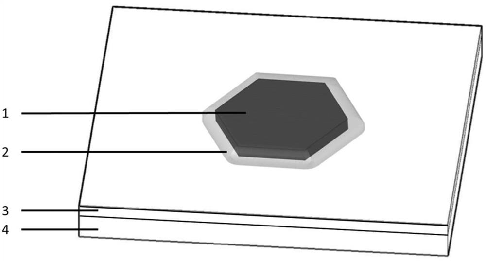
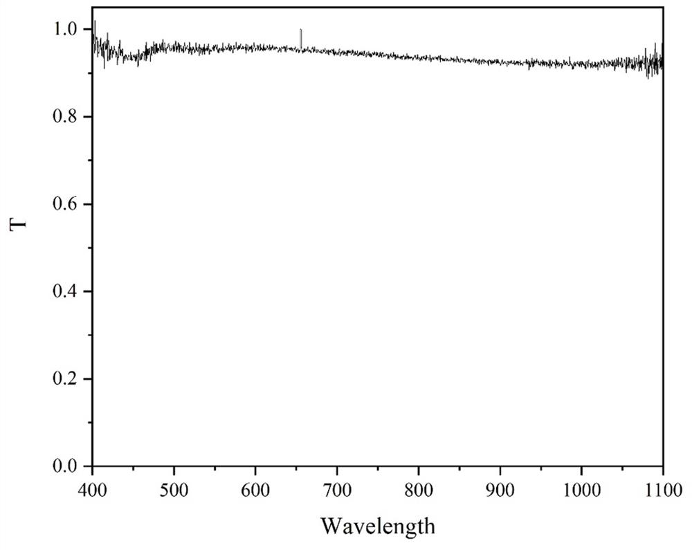
[0037] Specifically, as Figure 1~2 As shown, a high heat dissipation perovskite nanosheet laser according to an embodiment of the present invention includes: a thermally conductive base 4, on which a silicon dioxide bonding layer 3 is arranged, and the silicon dioxide bonding layer 3 is provided on the thermally conductive base 4. A perovskite nanosheet 1 is arranged on the composite layer 3 as a laser gain medium, a polyvinylidene fluoride (PVDF) encapsulation layer 2 is arranged above the perovskite nanosheet 1, and the polyvinylidene fluoride encapsulation layer 2 covers the Above and outside the perovskite nanosheet 1, the perovskite nanosheet 1 is encapsulated.
[0038] Specifically, in t...
Embodiment 2
[0050] The second embodiment of the present invention provides a preparation method of a perovskite nanosheet laser, which specifically includes the following preparation and implementation steps:
[0051] S1. Magnetron sputtering a layer of SiO on the surface of the diamond substrate 2 layer, specifically, SiO 2 The thickness of the layer is 200 nm and the surface roughness after coating is RMS < 2 nm.
[0052] S2. Using a two-step vapor deposition method, deposit MAPbI on the mica sheet 3 Nanosheets. Among them, the nanosheet surface roughness RMS<1 nm.
[0053] S3, then using the physical transfer method, transfer the target nanosheets from the mica sheet to the diamond-SiO prepared in step S1 2 On the substrate, the side length of the nanosheet is 40 μm and the thickness is 150 nm.
[0054] S4. Finally, at 50 °C, the PVDF powder was dissolved in N,N-dimethylformamide (DMF) to make a 10% (w / v) solution. in diamond-SiO 2 - Spin coating on the nanosheet at a high speed...
PUM
| Property | Measurement | Unit |
|---|---|---|
| Thickness | aaaaa | aaaaa |
| Surface roughness | aaaaa | aaaaa |
| Roughness | aaaaa | aaaaa |
Abstract
Description
Claims
Application Information


