
Three-terminal artificial synaptic device based on digital controllable printing ITO nanowire and preparation method of three-terminal artificial synaptic device

A technology of synaptic devices and nanowires, applied in the field of microelectronics, can solve the problems of high cost, complicated operation and cumbersome process of sputtering, and achieve the effects of stable chemical properties, simple process and low cost

Pending Publication Date: 2022-07-12
NANKAI UNIV
View PDF0 Cites 0 Cited by
  • Summary
  • Abstract
  • Description
  • Claims
  • Application Information

AI Technical Summary

Problems solved by technology

The document "Chitosan-Based Polysaccharide-Gated Flexible Indium Tin Oxide Synaptic Transistor with Learning Abilities" (see the American academic journal "ACS Applied Materials & Interfaces" 2018, Volume 10, pages 16881-16886), reports a method for preparing ITO by sputtering The method based on the three-terminal artificial synapse device, but the sputtering method has high cost, high energy consumption, cumbersome process and complicated operation

Method used


Image

  • Three-terminal artificial synaptic device based on digital controllable printing ITO nanowire and preparation method of three-terminal artificial synaptic device
  • Three-terminal artificial synaptic device based on digital controllable printing ITO nanowire and preparation method of three-terminal artificial synaptic device
  • Three-terminal artificial synaptic device based on digital controllable printing ITO nanowire and preparation method of three-terminal artificial synaptic device

Examples


Embodiment 1

[0036] (1) The Si / SiO 2 The substrates were ultrasonically cleaned with deionized water, isopropanol, acetone and anhydrous ethanol for 30 minutes, respectively, and then their surfaces were blown dry with nitrogen;

[0037] (2) Mix the two reagents with a mass ratio of N,N-dimethylformamide: anhydrous ethanol=20:1 to prepare a mixed solvent; mix the mass ratio of polyvinylpyrrolidone:indium nitrate hydrate=1:1.2, chlorine The reagent of stannous dihydrate:indium nitrate hydrate=1:6.5 is dissolved in the mixed solvent, and stirred with a magnetic stirrer at a temperature of 50 ° C for 6 hours to configure the precursor solution required for printing; in the precursor solution The mass concentration of polyvinylpyrrolidone is 10.4%;

[0038](3) using an electrofluidic printer to print the precursor solution configured in step (2) as ITO nanowires, wherein a high voltage of 0.65kV is applied on the syringe needle, and the distance from the syringe needle to the substrate is set...

Embodiment 2

[0046] (1) The Si / SiO 2 The substrates were ultrasonically cleaned with deionized water, isopropanol, acetone and anhydrous ethanol for 30 minutes respectively, and then the surfaces were blown dry with nitrogen gas;

[0047] (2) Mix the two reagents with a mass ratio of N,N-dimethylformamide: anhydrous ethanol=10:1 to prepare a mixed solvent; mix the mass ratio of polyvinylpyrrolidone:indium nitrate hydrate=1:2, chlorine Tin bisulfite dihydrate: indium nitrate hydrate = 1:10 reagent is dissolved in the mixed solvent, and stirred at a temperature of 40 ° C for 12 hours with a magnetic stirrer to configure the precursor solution required for printing; in the precursor solution The mass concentration of polyvinylpyrrolidone is 11%;

[0048] (3) Using an electrofluidic printer, the precursor solution configured in step (2) was printed as ITO nanowires, wherein a high voltage of 1.1 kV was applied on the syringe needle, the distance from the syringe needle to the substrate was se...

Embodiment 3

[0054] (1) The glass substrate was ultrasonically cleaned with deionized water, isopropanol, acetone and absolute ethanol for 30 minutes, and then the surface was dried with nitrogen;

[0055] (2) Mix the two reagents with a mass ratio of N,N-dimethylformamide: anhydrous ethanol=6:1 to prepare a mixed solvent; mix the mass ratio of polyvinylpyrrolidone:indium nitrate hydrate=1:2, chlorine Tin bisulfite dihydrate: indium nitrate hydrate = 1:20 reagent is dissolved in the mixed solvent, and stirred at 25°C for 12 hours with a magnetic stirrer to configure the precursor solution required for printing; in the precursor solution The mass concentration of polyvinylpyrrolidone is 9%;

[0056] (3) Using an electrofluidic printer, the precursor solution configured in step (2) was printed as ITO nanowires, wherein a high voltage of 1.3 kV was applied on the syringe needle, the distance from the syringe needle to the substrate was set to 4 mm, and the syringe needle was set to 4 mm. The...


PUM

PropertyMeasurementUnit
Diameteraaaaaaaaaa
Lengthaaaaaaaaaa
Thicknessaaaaaaaaaa

Abstract

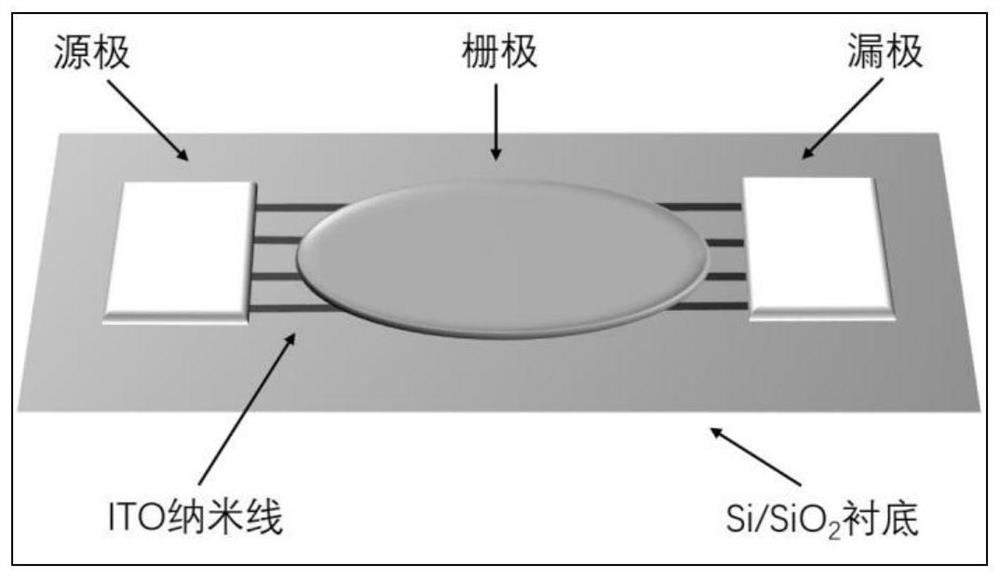
The invention relates to a three-terminal artificial synaptic device based on a digital controllable printing ITO (Indium Tin Oxide) nanowire and a preparation method of the three-terminal artificial synaptic device. According to the device, a nanowire array is distributed on a substrate, a source electrode and a drain electrode are distributed at the two ends of the array respectively, and ionic glue is arranged between the source electrode and the drain electrode to serve as a grid electrode; the preparation method comprises the following steps: firstly, preparing an ITO nanowire by using an electrofluid printer, and taking the ITO nanowire as a channel material of the synaptic device; then metal electrodes are evaporated on the ITO nanowire subjected to high-temperature annealing to serve as a source electrode and a drain electrode, and finally the three-terminal artificial synapse device is manufactured by using ionic gel as a grid electrode. The method is simple in process, easy and convenient to operate, low in cost, energy-saving, environment-friendly and suitable for large-scale production, and provides beneficial guidance for material selection and device design in the field of neuromorphic calculation.

Description

technical field [0001] The invention belongs to the field of microelectronics, in particular to a three-terminal artificial synapse device based on digitally controllable printing ITO nanowires and a preparation method thereof. Background technique [0002] In the 1950s, John McCarthy proposed the concept of artificial intelligence (AI), and with the successful manufacture of "AlphaGo", AI technology received more attention. At present, the implementation of AI is still based on the von Neumann architecture, which separates operation and storage, cannot achieve parallel computing, and has high power consumption. With the advent of the era of big data and artificial intelligence, a new computing system is urgently needed to replace the computing system of the von Neumann architecture. [0003] In a complex environment, the human brain can easily identify various objects through operations. It has lower power consumption, higher computing efficiency and fault tolerance than c...

Claims


Application Information

Patent Timeline
IPC IPC(8): H01L51/40H01L51/05B82Y40/00B82Y10/00
CPCB82Y10/00B82Y40/00H10K71/164H10K71/40H10K10/46Y02P70/50
Inventor 徐文涛屈尚达孙林
Owner NANKAI UNIV
Learn More