High-efficiency perovskite solar cell structure with double-interface processing and preparation method of high-efficiency perovskite solar cell structure
A solar cell and perovskite technology, applied in circuits, electrical components, photovoltaic power generation, etc., can solve the problem of low battery stability, and achieve the effects of improving stability, increasing scattering, and high efficiency
- Summary
- Abstract
- Description
- Claims
- Application Information
AI Technical Summary
Problems solved by technology
Method used
Image
Examples
preparation example Construction
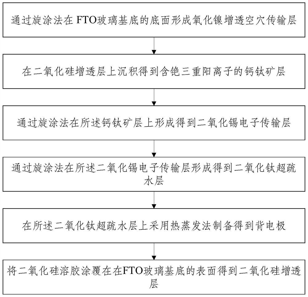
[0046] refer to figure 2 , the embodiment of the present application provides a preparation method of a double-interface treated high-efficiency perovskite solar cell structure, comprising the following steps:
[0047] S1. A nickel oxide antireflection hole transport layer is formed on the bottom surface of the FTO glass substrate by spin coating;
[0048] S2, depositing a perovskite layer containing cesium triple cations on the silica antireflection layer;
[0049] S3, forming a tin dioxide electron transport layer on the perovskite layer by a spin coating method;
[0050] S4, forming a titanium dioxide superhydrophobic layer on the tin dioxide electron transport layer by spin coating;
[0051] S5, preparing a back electrode by thermal evaporation on the superhydrophobic layer of titanium dioxide;
[0052] S6. Coat the silica sol on the surface of the FTO glass substrate to obtain a silica antireflection layer
[0053] In one embodiment, the described silica sol is coate...
Embodiment 1
[0071] Step 1: Dissolve 2.5g of nickel acetate tetrahydrate in 100ml of deionized water, stir for 12h, filter and spin at 3000rpm for 30s to the laser-etched FTO surface, and then sinter at 350°C for 1h to obtain nickel oxide Antireflection hole transport layer;
[0072] Step 2: Dissolve 548.6mg lead iodide, 77.1mg lead bromide, 190.1mg formamidine iodide and 21.8mg methylamine bromide in 0.8ml N,N-dimethylformamide and 0.2ml dimethylformamide In the mixed solvent of sulfoxide, 520 mg of cesium iodide and 1 mL of chloroform solution were then added, and the obtained mixed solution was stirred at room temperature for 1 h to be used as a perovskite precursor solution. Spin-coating the perovskite precursor solution, spin-coating the chlorobenzene anti-solvent on the surface of the precursor solution in the last 25 seconds, and then annealing at 100 °C for 60 min to obtain a cesium-containing triple cation perovskite layer;
Embodiment 2
[0077] Step 1: Dissolve 2.5g of nickel acetate tetrahydrate and 104mg of formamidine acetate in 100ml of deionized water, stir for 12h, filter and spin-coat at 3000rpm for 30 seconds on the laser-etched FTO surface, and then sinter at 400°C 1h to obtain a nickel oxide antireflection hole transport layer;
[0078] Step 2: Dissolve 548.6mg lead iodide, 77.1mg lead bromide, 190.1mg formamidine iodide and 21.8mg methylamine bromide in 0.8ml N,N-dimethylformamide and 0.2ml dimethylformamide In the mixed solvent of sulfoxide, 520 mg of cesium iodide and 1 mL of chloroform solution were then added, and the obtained mixed solution was stirred at room temperature for 1 h to be used as a perovskite precursor solution. Spin-coating the perovskite precursor solution, spin-coating the chlorobenzene anti-solvent on the surface of the precursor solution in the last 25 seconds, and then annealing at 100 °C for 60 min to obtain a cesium-containing triple cation perovskite layer;
[0079] The ...
PUM
| Property | Measurement | Unit |
|---|---|---|
| refractive index | aaaaa | aaaaa |
| refractive index | aaaaa | aaaaa |
| refractive index | aaaaa | aaaaa |
Abstract
Description
Claims
Application Information


