10 nano-level gap electrode preparing method

A nanoscale, electrode technology, applied in the direction of nanostructure manufacturing, nanotechnology, nanotechnology, etc., can solve the problems of easy to be affected by the external environment, unstable electrodes, unsuitable for industrial production, etc., to achieve easy control of parameters, nanometer The effect of stable electrode and low cost

Inactive Publication Date: 2004-09-15
UNIV OF SCI & TECH OF CHINA
View PDF0 Cites 7 Cited by
  • Summary
  • Abstract
  • Description
  • Claims
  • Application Information

AI Technical Summary

Problems solved by technology

Although this method can obtain nano-electrodes with precise interval widths, the electrodes are extremely unstable and easily affected by the external environment due to the need to keep the electrodes in an open state, and are not suitable for large-scale industrial production.

Method used


Image

  • 10 nano-level gap electrode preparing method
  • 10 nano-level gap electrode preparing method
  • 10 nano-level gap electrode preparing method

Examples


Embodiment 1

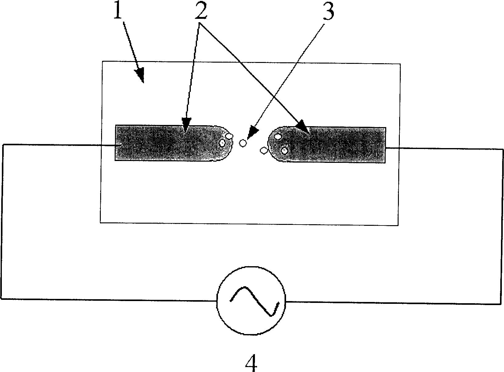
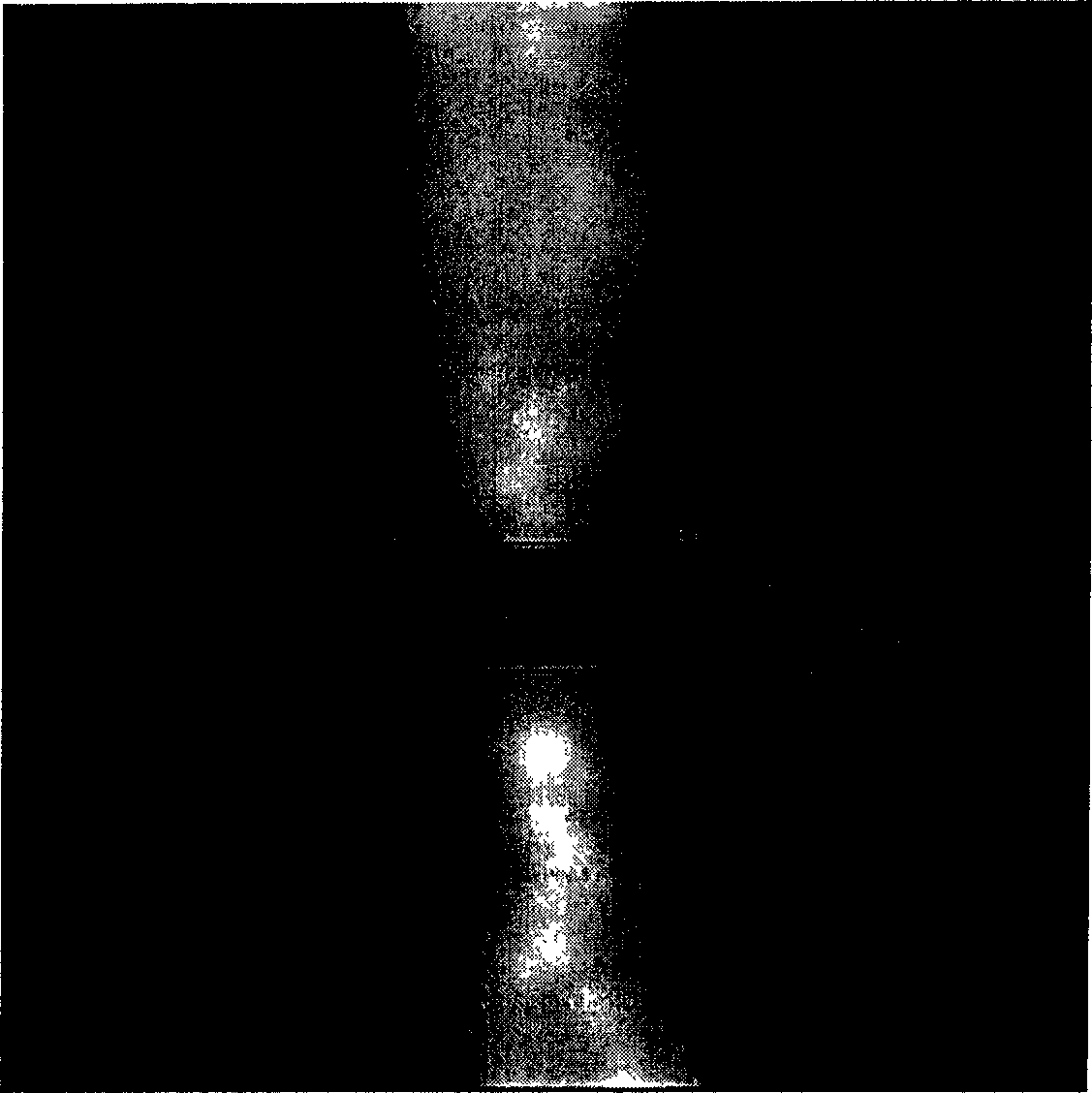
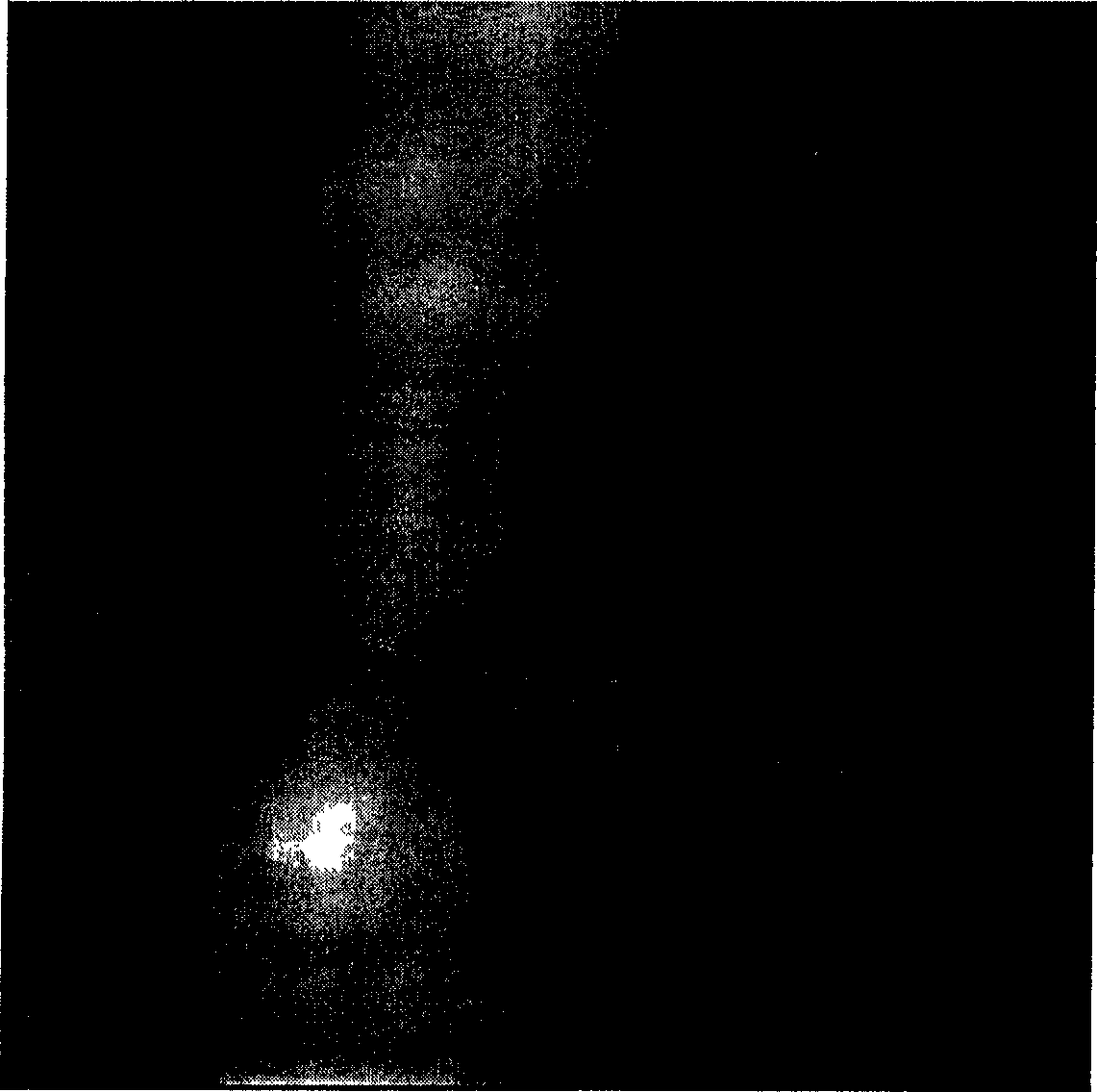
[0023] 1. Coating polymethyl methacrylate / poly(methyl methacrylate-methacrylamide) (PMMA / P(MMA-MAA)) double-layer glue on the silicon dioxide substrate 1 as an electron beam resist etchant; use the electron beam exposure method to etch grooves with a width and depth of about 200 nanometers on the surface of the double-layer glue, the electron beam acceleration voltage used is 20 kV, and the beam spot size is 0.1 micron; The evaporator evaporates gold with a thickness of about 15 nanometers on the surface, thereby depositing gold electrodes in the groove; when evaporating gold, the vacuum degree must be higher than 1.0×10 -3 Pa, control the temperature of the silicon dioxide substrate to be room temperature, and the thickness of the gold film on the evaporation can be controlled by a monitor; then use an ion beam etching machine to make polymethyl methacrylate / poly(methyl methacrylate-methacrylic acid) Dilute amide) double-layer glue is removed, promptly obtains gold electrode ...

Embodiment 2

[0031] 1, coat DNQ phenolic resin glue on the silicon dioxide substrate 1 as electron beam resist; Etch out the groove that width and depth are about 200 nanometers on this glue surface with electron beam exposure method, the adopted electron beam The accelerating voltage is 20 kV, and the beam spot size is 0.1 micron; then, a vacuum ion beam sputtering apparatus is used to grow platinum with a thickness of about 15 nanometers on the surface, thereby depositing a platinum electrode in the groove; the thickness of the platinum film can be monitored by instrument control; then use an ion beam etching machine to remove the DNQ phenolic resin glue to obtain the platinum electrode 2;

[0032] 2. Oxygen flame burns the surface of the platinum electrode prepared above, then puts it into an acetone solution for cleaning, removes organic impurities such as residual photoresist, and obtains a clean platinum electrode 2; the interval between the platinum electrodes is 300 nanometers;

[...


PUM


Abstract

The preparing method includes steps: (1) preparing metal electrode by using method of electronbeam exposure, removing organic matter from prepared metal electrode, interval of electrodes is as 50-300 Nano; (2) preparing suspension liquid of gold granule in size 5-50 Nano; (3) diluting suspension liquid prepared by using water till particle concentration is 1012-1014 pieces / cubic centimeter, dropping suspension liquid diluted onto surface of metal electrode prepared at step (1); applying AC voltage to two ends of electrode, then blowing drying surface by using inactive gas; (4) carrying out low temperature annealing treatment for electrode obtained from step (3). Advantages of the method are: simple technique, easy of controlling parameters. Nano electrode prepared by using the method is very stable, shape of the electrode is not easy to change, the product is suitable to use in industrial.

Description

technical field [0001] The invention relates to a processing method of a nanometer device, in particular to a preparation method of a 10 nanometer device Background technique [0002] With the development of the semiconductor industry and large-scale integrated circuits, the number of devices that can be accommodated per unit area reaches 10 9 Every square centimeter, the size of a single semiconductor device is getting smaller and smaller. By 2002, the line width could be 0.2 microns. The development of the entire semiconductor industry has entered the submicron era and is moving towards the nanometer era. With the deepening of research on nanodevices, especially molecular devices, people need a good and stable way to connect the two ends of nanodevices, commonly known as nanoelectrodes. A stable nanoelectrode with an interval of 10 nanometers or even smaller is essential for people to explore and study the nanoworld. [0003] The U.S. "Applied ...

Claims


Application Information

Patent Timeline
Patent Type & Authority Applications(China)
IPC IPC(8): B82B3/00H01L21/28H01L21/44
Inventor 张琨王振兴王晓平侯建国
Owner UNIV OF SCI & TECH OF CHINA
Why Eureka
Try Eureka