Flash memory structure and its preparation method

A memory unit and flash technology, applied in semiconductor/solid-state device manufacturing, semiconductor devices, electric solid-state devices, etc., can solve problems such as poor injection efficiency, difficulty in controlling the coupling capacitance of floating gate and control gate, and low programming efficiency , to achieve process compatibility, improve programming injection efficiency, and simple preparation method

A memory unit and flash technology, applied in semiconductor/solid-state device manufacturing, semiconductor devices, electric solid-state devices, etc., can solve problems such as poor injection efficiency, difficulty in controlling the coupling capacitance of floating gate and control gate, and low programming efficiency , to achieve process compatibility, improve programming injection efficiency, and simple preparation method

CN1805146AActive Publication Date: 2006-07-19PEKING UNIV +1

Image

  • Flash memory structure and its preparation method
  • Flash memory structure and its preparation method
  • Flash memory structure and its preparation method

Examples


Embodiment 1

[0040] Embodiment 1: Flash memory cell with self-aligned split gate floating gate structure based on vertical channel field effect transistor

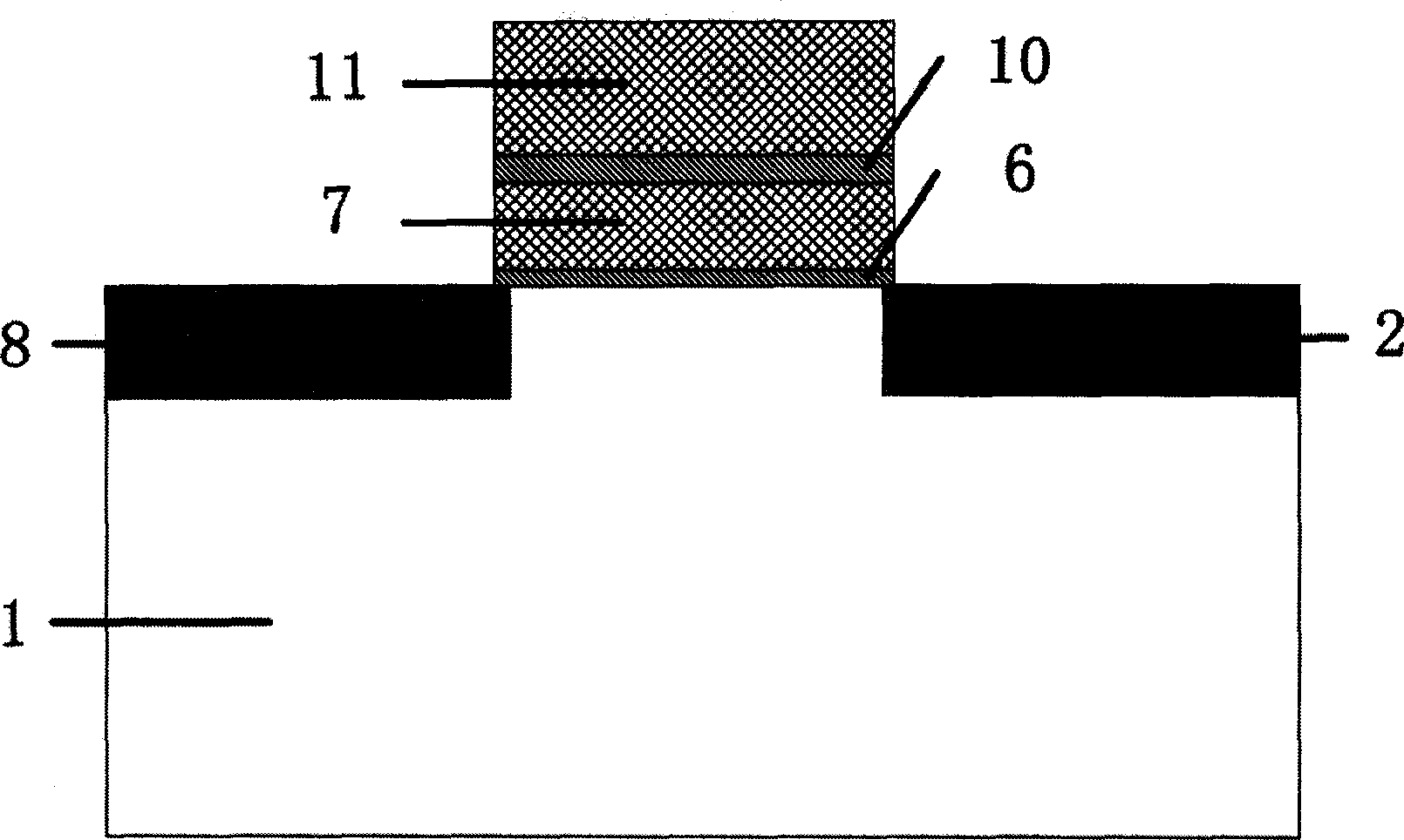
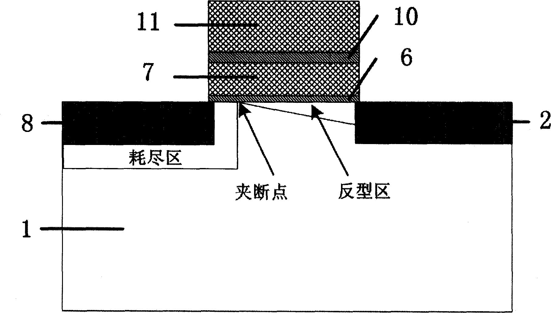
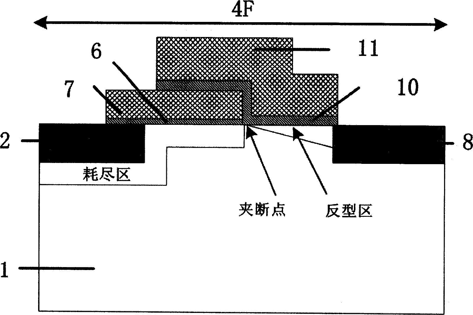
[0041] Such as Figure 5 As shown, it is the flash memory unit of this embodiment, wherein, the silicon substrate 1, that is, the top of the silicon platform is a silicon nitride hard mask 4 and a silicon dioxide hard mask 3, and the n+ doped region above the silicon platform It is the source terminal 2, and its junction depth is 2500 angstroms. Such a deep junction depth is to increase the coupling capacitance between the source terminal and the floating gate, so as to improve the programming injection efficiency. The n+ doped regions on both sides of the silicon platform are drain terminals 8, and the junction depth is 1000 angstroms. There are two polysilicon gates on both sides of the silicon platform. The outer polysilicon gate is a control gate 11 with a horizontal thickness of 500 angstroms; the inner polysilicon gate is a floa...

Embodiment 2

[0044] Embodiment 2: A preparation method of a flash memory unit

[0045] As shown in FIG. 7 , the products of each step shown in FIG. 7 ( 1 )-( 8 ) correspond to each step in a method for preparing the flash memory unit described in the previous embodiment. The method is described in detail below in conjunction with the product of each step:

[0046] (1). Single throwing p-type bulk silicon substrate 1, shallow trench isolation (STI), implanting boron for adjusting the threshold and implanting arsenic for source doping, forming a structure as shown in Figure 7 (1) (the figure only shows The source part, the same below), the source 2 junction depth of the device finally formed is 2500 angstroms;

[0047] (2). Deposit silicon dioxide 300 angstroms and silicon nitride 1200 angstroms, photolithographic device silicon plate, anisotropic etching silicon nitride and silicon dioxide to form double-layer hard masks 3 and 4, as shown in Figure 7 (2) );

[0048] (3). Using ICP with h...


PUM

PropertyMeasurementUnit
Thicknessaaaaaaaaaa

Abstract

The invention relates to a quick flash memory unit, which is based on the vertical-channel fieldistor. It is characterized in that: the n+ doping area above the silicon base is the source; the n+ doping area at the two sides of silicon base are leak ends; the each side of silicon base has two multi-silicon grids, while the outer multi-silicon grid is the control grid and the inner multi-silicon grid is the float grid; the spaces between the float grid and the channel area and the source area are the tunnel oxygenation layers; the spaces between the control grid and the channel area and the float grid are the baffle oxygenation layers; the n+ leak ends at the two sides of silicon base are separated connected to form two memory units sharing the source end. The invention also provides a preparation method of said device, which is characterized in that: it uses the plasma coupling high-selection rate opposite etching technique and the reaction ion hermaphroditic etching technique, to self-position form the separation grid and float grid structures, while the channel length of control grid and the channel length of float grid are both realized by the etching technique.

Description

technical field [0001] The invention belongs to the technical field of non-volatile semiconductor memory, and relates to a flash memory unit and a preparation method thereof, in particular to a flash memory unit with a split gate floating gate structure based on a vertical channel field effect transistor and a preparation method thereof. Background technique [0002] Semiconductor memory is an important part of the semiconductor industry. With the increasing demand for data storage in various mobile devices, the demand for non-volatile semiconductor memory that can still store data in the event of power failure is also increasing. Flash memory (flash memory, referred to as flash memory) is the fastest growing non-volatile semiconductor memory. Since the first flash memory product came out in the 1980s, with the development of technology, it has been widely used in mobile communication devices and personal computers such as mobile phones, notebook computers, handheld computer...

Claims


Application Information

Patent Timeline
19 Jul 2006
Publication
CN1805146A
IPC
H01L27/115; H01L21/8247; H01L27/11521
Inventors
周发龙; 黄如